Semiconductor memory device having wiring line structure

a memory device and three-dimensional structure technology, applied in semiconductor devices, semiconductor/solid-state device details, electrical apparatus, etc., can solve the problem of complex achieve the effect of improving the structure of wiring lines, reducing the area required by wiring structures, and improving wiring lines

Active Publication Date: 2021-12-07
SK HYNIX INC
View PDF3 Cites 1 Cited by
  • Summary
  • Abstract
  • Description
  • Claims
  • Application Information

AI Technical Summary

Benefits of technology

[0004]The present invention in its broadest aspects relates to a semiconductor memory device of a three-dimensional structure having an improved wiring line structure. One advantage of the improved wiring line structure is that it reduces the area required by the wiring structure, thus allowing more area of the semiconductor device to be used for storing data. In an embodiment, a semiconductor memory device may include: a first substrate including first, second, and third regions arranged adjacent sequentially adjacent to each other along a first direction; a memory block including a plurality of electrodes and interlayer dielectric layers alternately stacked over the first substrate; a slit dividing the memory block into a first electrode structure and a second electrode structure in the second region; and a plurality of step-shaped grooves formed to different depths in the memory block in the second region, the plurality of the step-shaped grooves being divided by the slit. The first electrode structure and the second electrode structure may be disposed adjacent to each other in a second direction intersecting with the first direction with the slit interposed therebetween. Each of the electrodes of the first electrode structure may have a first pad region which is exposed by another electrode positioned thereon, in any one of the step-shaped grooves, each of the electrodes of the second electrode structure may have a second pad region which is exposed by another electrode positioned thereon, in any one of the step-shaped grooves, and first pad regions of the first electrode structure and second pad regions of the second electrode structure which are positioned in the same step-shaped groove and are disposed at the same layers may be disposed adjacent to each other in the second direction with the slit interposed therebetween.

Problems solved by technology

Also, the structure of the wiring lines becomes more complex.

Method used


Image

  • Semiconductor memory device having wiring line structure
  • Semiconductor memory device having wiring line structure
  • Semiconductor memory device having wiring line structure

Examples


Embodiment Construction

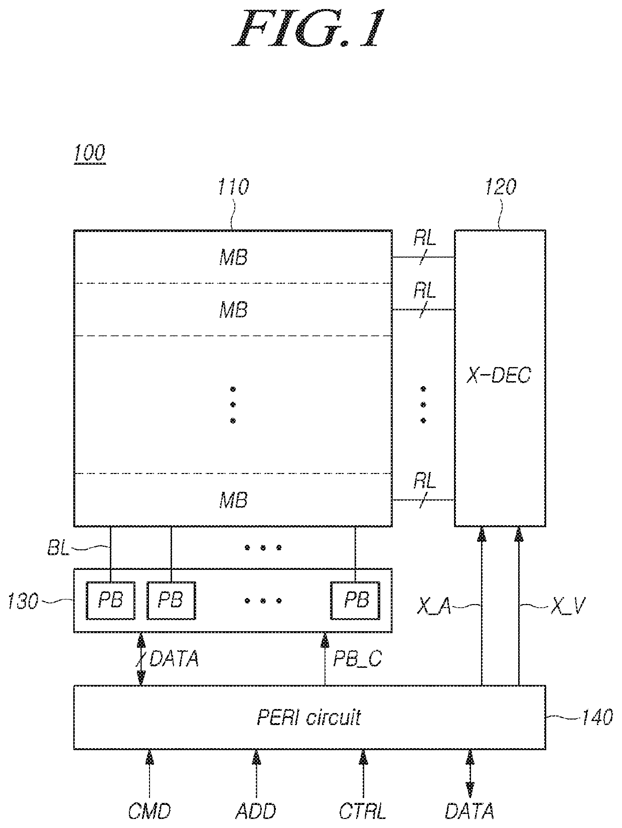
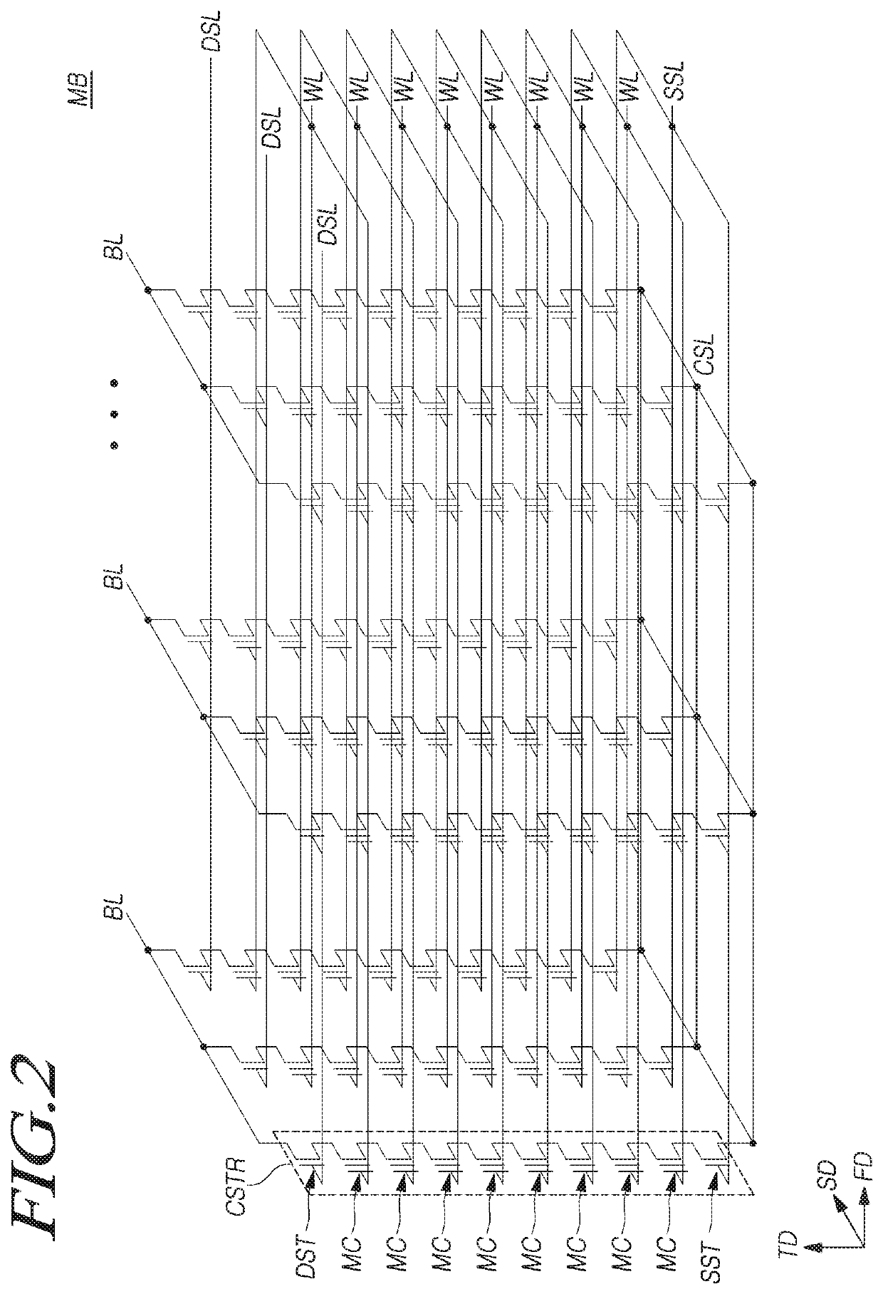
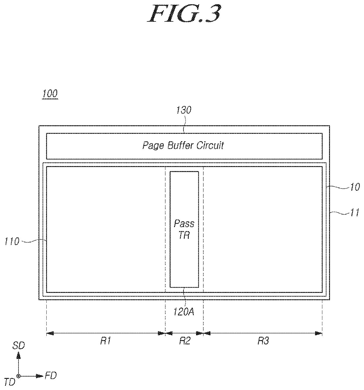
[0032]Advantages and features of the present invention will become apparent from the following descriptions of various embodiments with reference to the accompanying drawings. However, the disclosure is not limited to the embodiments disclosed herein but may be implemented in various different ways. The embodiments are provided for making the disclosure of the disclosure thorough and for fully conveying the scope of the disclosure to those skilled in the art to which the disclosure pertains. It is to be noted that the scope of the disclosure is defined only by the claims.

[0033]The figures, dimensions, ratios, angles, numbers of elements given in the drawings to describe embodiments of the disclosure are merely illustrative and are not limiting. Throughout the specification, like reference numerals refer to like elements. In describing the disclosure, when it is determined that the detailed description of the known related art may obscure the gist of the disclosure, the detailed desc...


PUM

PropertyMeasurementUnit
depthsaaaaaaaaaa
widthaaaaaaaaaa
structureaaaaaaaaaa

Abstract

A semiconductor memory device includes a substrate having a second region extending in a first direction; a memory block including electrodes; a slit dividing the memory block into first and second electrode structures in the second region; and step-shaped grooves formed in the memory block in the second region, and divided by the slit. In the second region, the first and second electrode structures are adjacently disposed with the slit interposed therebetween, in a second direction intersecting with the first direction. Each of the electrodes of the first electrode structure has a first pad region, each of the electrodes of the second electrode structure has a second pad region, and first and second pad regions of the first and second electrode structures which are positioned in the same step-shaped groove and are disposed at the same layers are adjacently disposed in the second direction with the slit interposed therebetween.

Description

CROSS-REFERENCE TO RELATED APPLICATION[0001]The present application claims priority to Korean Patent Application No. 10-2019-0035753 filed on Mar. 28, 2019, in the Korean Intellectual Property Office, which is incorporated herein by reference in its entirety.BACKGROUND1. Technical Field[0002]Various embodiments of the present invention generally relate to a semiconductor memory device of a three-dimensional structure and, more particularly, to a semiconductor memory device of a three-dimensional structure having an improved wiring line structure.2. Related Art[0003]Generally, as semiconductor memory devices trend toward larger capacity and higher degree of integration, the number of the required wiring lines included in the semiconductor memory device for the operation and electrical coupling of the semiconductor memory device increases. Also, the structure of the wiring lines becomes more complex. At the same time, the area allocated for the layout of the wiring lines is decreasing...

Claims


Application Information

Patent Timeline
Patent Type & Authority Patents(United States)
IPC IPC(8): H01L27/11582H01L25/18H01L23/522H01L23/528H01L27/11573H01L23/00H01L27/11575H01L27/11565H01L27/1157
CPCH01L27/11582H01L23/528H01L23/5226H01L24/08H01L25/18H01L27/11565H01L27/11573H01L27/11575H01L27/1157H01L2224/08145H01L2924/1431H01L2924/14511H10B43/27H01L27/0688H10B43/10H10B43/35H10B43/40H10B43/50
Inventor OH, SUNG LAEKIM, JIN HOSUNG, SANG HYUNKIMJEON, BYUNG HYUN
Owner SK HYNIX INC
Why Eureka
Try Eureka