Optical structure
a technology of optical structure and optical axis, applied in the field of optical structure, can solve the problem of large optical structure, and achieve the effect of easy adjustmen
- Summary
- Abstract
- Description
- Claims
- Application Information
AI Technical Summary
Benefits of technology
Problems solved by technology
Method used
Image
Examples
first embodiment
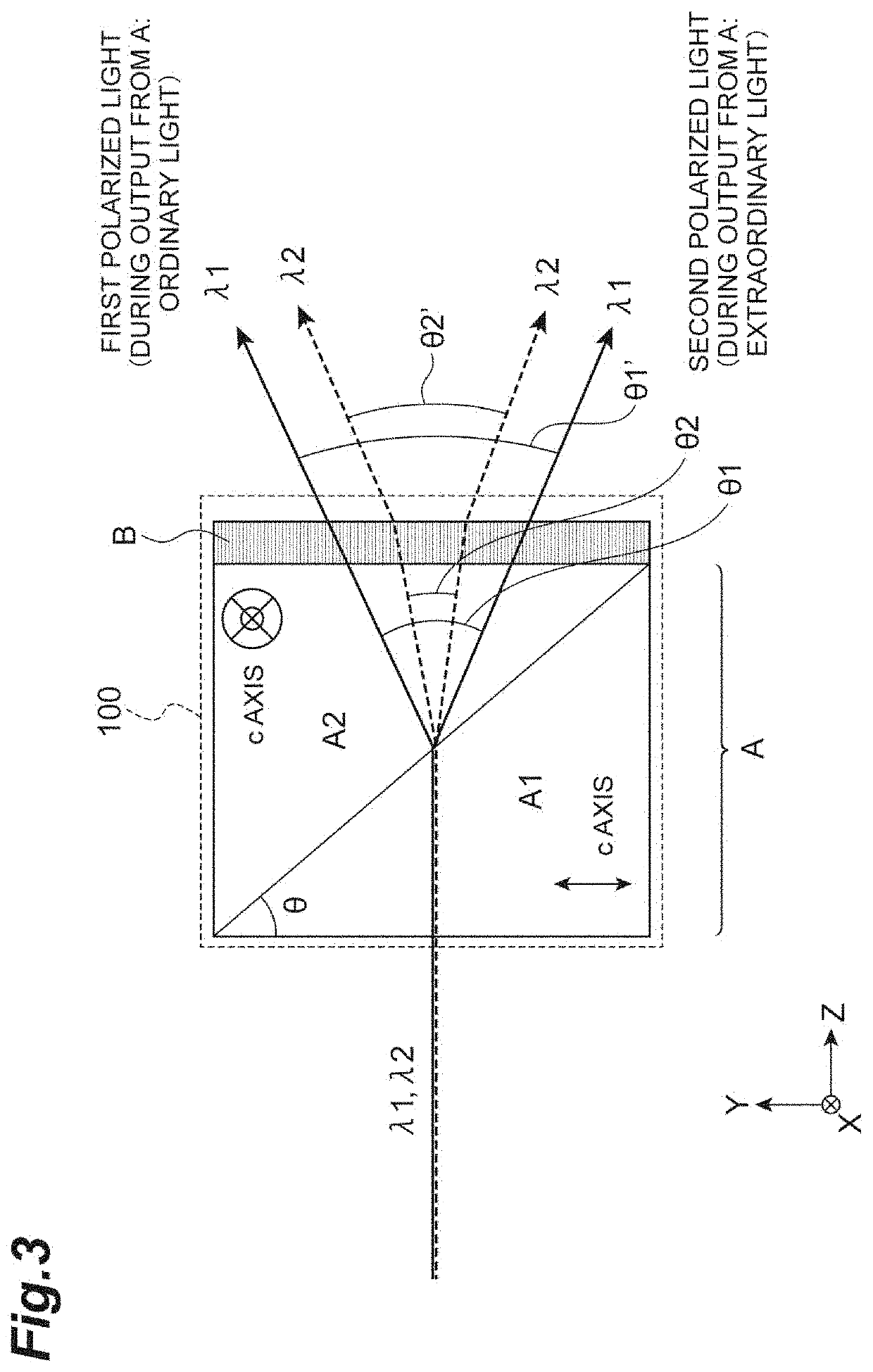
[0041]FIG. 3 is a diagram illustrating an optical structure according to a
[0042]An optical structure 100 includes a polarizing beam splitter A that splits input light input from an incoming plane into first polarized light and second polarized light, and diffractive optical element B (diffraction means: a diffraction grating or a spatial light modulator) that is disposed at a stage subsequent to the polarizing beam splitter A and has a plurality of light transmission regions separated at a prescribed pitch. Split angles in the polarizing beam splitter A, which are angles formed by the traveling directions of the rays of first polarized light and by the traveling directions of the rays of the second polarized light, are acute angles. The diffractive optical element B of FIG. 3 is a diffraction grating, but it may be a spatial light modulator. that displays a diffraction grating pattern.
[0043]When first input light having a first wavelength λ1 is input to the polarizing beam splitter ...
second embodiment
[0065]FIG. 6 is a diagram illustrating an optical structure according to a
[0066]In this optical structure 100, the polarizing beam splitter A and the diffractive optical element B are integrated without a junction plane. The optical structure 100 of FIG. 6 is different from that illustrated in FIG. 3 only in this respect, and is the same in other respects.
[0067]In the case of this configuration, there are effects that it is not necessary to adhere the diffractive optical element B to the Wollaston prism, an angle deviation at the time of adhesion between the diffractive optical element and the polarizing beam splitter is minimized, and a loss of light or the like resulting from a refractive index difference between an adhesive and a member is minimized. The diffractive optical element B is a diffraction grating, and a structure thereof is as described above.
third embodiment
[0068]FIG. 7 is a diagram illustrating an optical structure according to a
[0069]This optical structure 100 includes first diffractive optical element B1 and second diffractive optical element B2. In the case of the present example, a structure of each diffractive optical element is identical to those illustrated in FIGS. 5A and 5B. To be specific, the diffractive optical element B includes the first diffractive optical element B1 having a first pattern made up of some of the plurality of light transmission regions R, and the second diffractive optical element having a second pattern made up of the others of the plurality of light transmission regions. The first diffractive optical element B1 and the second diffractive optical element B2 may be in contact with each other, be separated from each other, or form both the patterns with the same member.
[0070]The first polarized light of the first input light (of the first wavelength λ1) and the first polarized light of the second input li...
PUM
| Property | Measurement | Unit |
|---|---|---|
| wavelength | aaaaa | aaaaa |
| wavelength | aaaaa | aaaaa |
| optical structure | aaaaa | aaaaa |
Abstract
Description
Claims
Application Information
 - R&D
- Intellectual Property
- Life Sciences
- Materials
- Tech Scout
- Unparalleled Data Quality
- Higher Quality Content
- 60% Fewer Hallucinations
Browse by: Latest US Patents, China's latest patents, Technical Efficacy Thesaurus, Application Domain, Technology Topic, Popular Technical Reports.
© 2025 PatSnap. All rights reserved.Legal|Privacy policy|Modern Slavery Act Transparency Statement|Sitemap|About US| Contact US: help@patsnap.com


