Semiconductor device having crystal defects and method of manufacturing the semiconductor device having crystal defects

a semiconductor device and crystal defect technology, applied in semiconductor devices, diodes, electrical devices, etc., can solve the problems of more prone to oscillation and liable to generate oscillation, and achieve the effect of shortening the reverse recovery time, shortening the reverse recovery charge amount, and increasing the switching speed

Active Publication Date: 2020-10-27
SHINDENGEN ELECTRIC MFG CO LTD
View PDF11 Cites 1 Cited by
  • Summary
  • Abstract
  • Description
  • Claims
  • Application Information

AI Technical Summary

Benefits of technology

[0032]According to the semiconductor device of the present invention, the crystal defects whose density is increased locally as viewed along a depth direction are formed in the n-type column region and the p-type column region. With such a configuration, in the same manner as the conventional semiconductor devices, carriers can be recoupled at the crystal defects (a lifetime of carriers can be controlled) at the time of reverse recovery of a body diode. As a result, the carriers can be recovered even when the carriers do not move to an electrode. Accordingly, in the semiconductor device of the present invention, a switching speed can be increased by shortening a reverse recovery time (Trr). As a result, a reverse recovery charge amount (Qrr) can be reduced thus providing a semiconductor device which can reduce a recovery loss.
[0033]According to the semiconductor device of the present invention, the relationship of 0.25Dp≤Dd<0.95Dp and the relationship of 0.05Dp<W<0.5Dp (particularly, 0.25Dp≤Dd<0.95Dp) are satisfied. Accordingly, compared to the conventional semiconductor devices, a time until carriers existing in the vicinity of the deepest portion of the super junction structure are recoupled becomes relatively long and hence, it is possible to suppress a rapid growth of a depletion layer from a pn junction at the time of reverse recovery of the body diode. As a result, according to the semiconductor device of the present invention, it is possible to suppress the occurrence of a phenomenon that a reverse recovery current (Irr) becomes rapidly small (dIr / dt becoming large) after the reverse recovery current (Irr) passes a peak value (Irp). Accordingly, it is possible to suppress the increase of an induced electromotive force generated by a parasitic inductance component. As a result, the semiconductor device according to the present invention becomes a semiconductor device where oscillation is not easily generated compared to conventional semiconductor devices.
[0034]Accordingly, the semiconductor device of the present invention becomes a semiconductor device which can reduce a recovery loss and in which oscillation is not easily generated compared to conventional semiconductor devices.
[0035]According to the method of manufacturing a semiconductor device according to the present invention, in the crystal defect forming step, the crystal defects are formed such that, using the first main surface as a reference, a relationship of 0.25Dp≤Dd<0.95Dp and a relationship of 0.05Dp<W<0.5Dp are satisfied. Accordingly, it is possible to manufacture a semiconductor device which can reduce a recovery loss and in which oscillation is not easily generated compared to conventional semiconductor devices as described previously.
[0036]The present invention is applicable to various semiconductor devices which use a super junction structure. However, the present invention is most suitably applicable to a MOSFET.

Problems solved by technology

That is, a MOSFET having a super junction structure has a drawback that oscillation is liable to be generated, and a MOSFET where crystal defects are formed as in the case of the conventional MOSFET 900 has a drawback that oscillation is more liable to be generated.

Method used


Image

  • Semiconductor device having crystal defects and method of manufacturing the semiconductor device having crystal defects
  • Semiconductor device having crystal defects and method of manufacturing the semiconductor device having crystal defects
  • Semiconductor device having crystal defects and method of manufacturing the semiconductor device having crystal defects

Examples


embodiment 1

1. Configuration of Semiconductor Device (MOSFET 100)

[0055]Firstly, the semiconductor device according to the embodiment 1 is described.

[0056]The semiconductor device according to the embodiment 1 is an MOSFET, and the MOSFET is described hereinafter as a MOSFET 100.

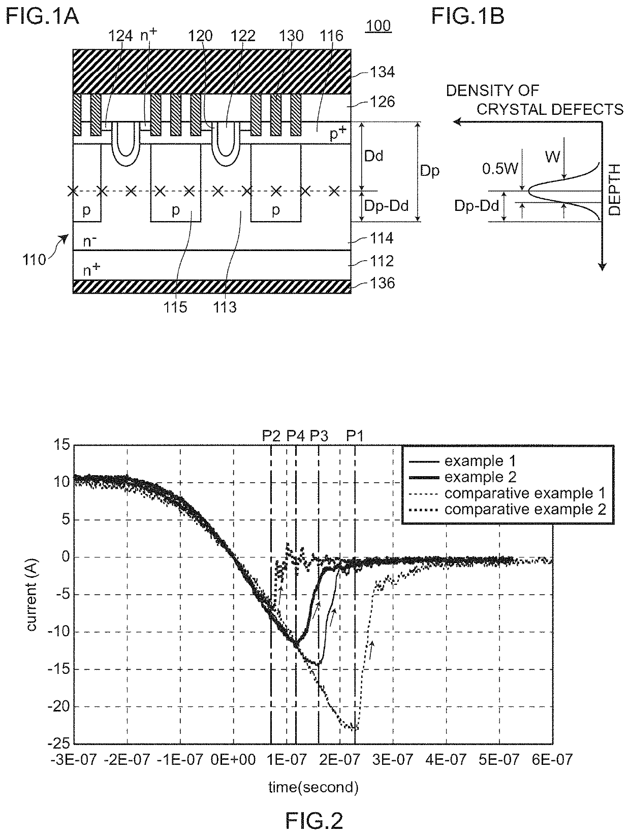
[0057]As shown in FIG. 1A, the MOSFET 100 according to the embodiment 1 is a MOSFET which includes: a semiconductor base substrate 110 which has n-type column regions 113 and p-type column regions 115 and in which a super junction structure is formed of the n-type column regions 113 and the p-type column regions 115; and gate electrodes 122 which are formed on a first main surface side of the semiconductor base substrate 110 by way of gate insulation films 120. A drain-source withstand voltage of the MOSFET 100 is 300 V or more and is 600 V, for example.

[0058]In this specification, “super junction structure” means a structure where n-type column regions and p-type column regions are arranged alternately in a repeated man...

embodiment 2

[0160]A MOSFET 101 according to the embodiment 2 basically has substantially the same configuration as the MOSFET 100 according to the embodiment 1. However, the MOSFET 101 according to the embodiment 2 differs from the MOSFET 100 according to the embodiment 1 with respect to a depth at which density of crystal defects exhibits a maximum value. That is, in the MOSFET 101 according to the embodiment 2, as shown in FIG. 7A and FIG. 7B, a depth Dd at which density of crystal defects exhibits a maximum value is smaller than the corresponding depth in the MOSFET 100 according to the embodiment 1. The depth Dd at which density of crystal defects exhibits a maximum value in the MOSFET 101 is specifically 0.25Dp.

[0161]In the MOSFET 101 according to the embodiment 2, Dd is 0.25Dp. Accordingly, a relationship of 0.25Dp≤Dd<0.95Dp is satisfied and a relationship of Dd≤0.5Dp is also satisfied. As a matter of course, the above-mentioned “Dd is 0.25Dp” is described for an exemplifying purpose. Fro...

embodiment 3

[0168]A MOSFET 102 according to the embodiment 3 basically has substantially the same configuration as the MOSFET 100 according to the embodiment 1. However, the MOSFET 102 according to the embodiment 3 differs from the MOSFET 100 according to the embodiment 1 with respect to a depth at which density of crystal defects exhibits a maximum value. That is, in the MOSFET 102 according to the embodiment 3, as shown in FIG. 8A and FIG. 8B, the depth Dd at which density of crystal defects exhibits a maximum value is deeper than the corresponding depth Dd in the MOSFET 100 according to the embodiment 1. In the MOSFET 102, the depth Dd at which density of crystal defects exhibits a maximum value is specifically 0.9Dp.

[0169]The MOSFET 102 according to the embodiment 3 does not satisfy a condition of (Dp−Dd)>0.5W. However, depending on the configuration of the semiconductor device (MOSFET), there is a case where the MOSFET 102 having such a configuration can also acquire a sufficient advantage...


PUM

PropertyMeasurementUnit
temperatureaaaaaaaaaa
voltageaaaaaaaaaa
voltageaaaaaaaaaa

Abstract

A MOSFET includes: a semiconductor base substrate having n-type column regions and p-type column regions, the n-type column regions and the p-type column regions forming a super junction structure; and a gate electrode which is formed on a first main surface side of the semiconductor base substrate by way of a gate insulation film, wherein crystal defects whose density is increased locally as viewed along a depth direction are formed in the n-type column regions and the p-type column regions, using the first main surface as a reference and assuming a depth to a deepest portion of the super junction structure as Dp, a depth at which density of the crystal defects exhibits a maximum value as Dd, and a half value width of density distribution of the crystal defects as W, a relationship of 0.25Dp≤Dd<0.95Dp and a relationship of 0.05Dp<W<0.5Dp are satisfied.

Description

RELATED APPLICATIONS[0001]The present application is a Continuation-in-part application of PCT international application No. PCT / JP2018 / 009591 filed on Mar. 12, 2018, which claims priority from International Application No. PCT / JP2017 / 039640 filed Nov. 1, 2017, the disclosures of which are hereby incorporated by reference herein in their entirety.BACKGROUND OF THE INVENTION1. Field of the Invention[0002]The present invention relates to a semiconductor device and a method of manufacturing a semiconductor device.2. Description of the Related Art[0003]Conventionally, with respect to a MOSFET which uses a super junction structure, there has been known a MOSFET where crystal defects are formed by He irradiation (see JR 2015-135987 A, for example)[0004]As shown in FIG. 17, the conventional MOSFET 900 includes a semiconductor base substrate 910 which has n-type column regions 913 and p-type column regions 915 and in which a super junction structure is formed of the n-type column regions 91...

Claims


Application Information

Patent Timeline
Patent Type & Authority Patents(United States)
IPC IPC(8): H01L21/22H01L29/78H01L29/10H01L29/32H01L29/66H01L29/06H01L21/324
CPCH01L29/1095H01L29/66734H01L29/7805H01L21/221H01L29/7813H01L29/0634H01L21/324H01L29/32H01L21/26506H01L29/41766H01L29/66712H01L29/7802
Inventor ARAI, DAISUKEKITADA, MIZUEASADA, TAKESHISUZUKI, NORIAKIMURAKAMI, KOICHI
Owner SHINDENGEN ELECTRIC MFG CO LTD
Why Eureka
Try Eureka