Gate clock generator and display device having the same

a display device and generator technology, applied in the direction of instruments, static indicating devices, etc., can solve the problems of limitation of gate pulses applied to the lines of display panels, same phase and same pulse width

Active Publication Date: 2020-10-20
LG DISPLAY CO LTD
View PDF3 Cites 3 Cited by
  • Summary
  • Abstract
  • Description
  • Claims
  • Application Information

AI Technical Summary

Benefits of technology

[0005]A gate clock generator of the present disclosure includes a counter, a buffer control signal generator, and an output unit. The counter receives control data having rising timing information and falling timing information and a main clock, generates a first output when a value obtained by counting the main clock from a preset reference time point reaches rising data, and generates a second output when a value obtained by counting the main clock from the reference time point reaches falling data. The buffer control signal generator generates a first buffer control signal of a gate ON voltage from a timing of the first output to a timing of the second output. The output unit outputs a gate ON voltage of a gate clock during an output period of the gate ON voltage of the first buffer control signal.

Problems solved by technology

In particular, since each of the gate clocks output from the level shifter is sequentially shifted, the gate pulses applied to the lines of the display panel have a limitation that they have the same phase and the same pulse width.

Method used


Image

  • Gate clock generator and display device having the same
  • Gate clock generator and display device having the same
  • Gate clock generator and display device having the same

Examples


first embodiment

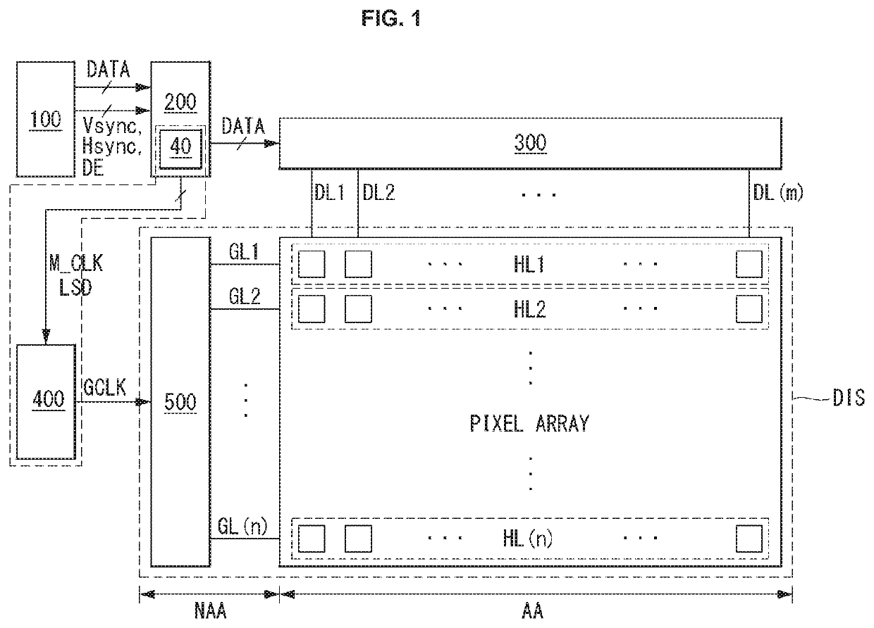
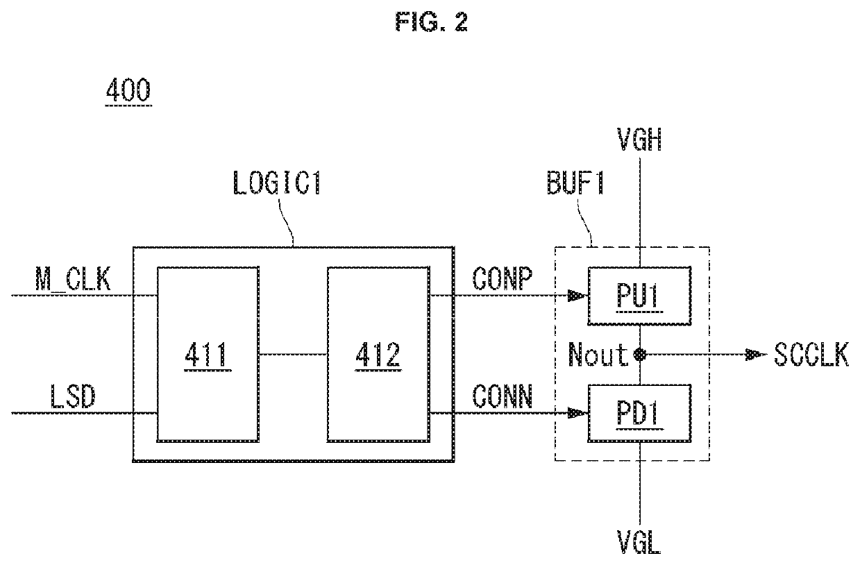
[0045]Referring to FIGS. 2 to 4, the gate clock generator 400 includes a logic unit LOGIC1 and a buffer unit BUF 1.

[0046]The logic unit LOGIC1 receives the main clock M_CLK and the control data LSD and generates a buffer control signal on the basis of the main clock M_CLK and the control data LSD. To this end, the logic unit LOGIC1 includes a counter 411 and a buffer control signal generator 412. In one or more embodiments, the term “unit” used herein may be broadly construed to be a circuit, a module of an electronic system, a subsystem or a system implemented using electronic circuitry, one or more functioning unit structure of a larger system, or the like.

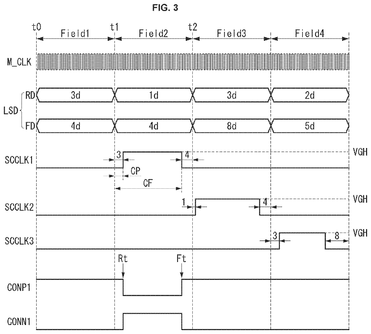
[0047]The counter 411 receives the main clock M_CLK and the control data LSD and counts the main clock M_CLK according to information of the control data LSD belonging to one field to adjust a timing of first and second buffer control signals CONP and CONN.

[0048]Each of the fields Field1 to Field4 may be set to a period for dri...

second embodiment

[0062]As illustrated in FIG. 5, the gate clock generator 400 includes a logic unit LOGIC2, first and second multiplexers MUX1 and MUX2, and a buffer unit BUF2.

[0063]The logic unit LOGIC2 includes a counter 411, a buffer control signal generator 412, and a multiplexer controller 414. The counter 411 and the buffer control signal generator 412 included in the logic unit LOGIC2 may have the same configuration and perform the same operation as those of the first embodiment described above. That is, although not shown in FIG. 6, the logic unit LOGIC2 according to the second embodiment may output the first buffer control signal CONP and the second buffer control signal CONN on the basis of the rising data RD and the falling data FD illustrated in FIG. 3. The multiplexer controller 414 adjusts the number of switches to be turned on included in the first and second multiplexers MUX1 and MUX2 on the basis of slew rate control data SD of the control data LSD. The operation of the multiplexer...

third embodiment

[0077]The gate clock generator will be described with reference to FIGS. 11 to 13.

[0078]The gate clock generator LS3 according to the third embodiment includes a logic unit LOGIC 3 and a buffer unit BUF 3.

[0079]The logic unit LOGIC 3 includes a counter 411, a buffer control signal generator 412, a GPM control signal generator 415, and a GPM controller 416.

[0080]The counter 411 and the buffer control signal generator 412 of the logic unit LOGIC 3 may have the same configuration and perform the same operation as those of the first embodiment described above. That is, although rising data and falling data are not shown in FIG. 11, the logic unit LOGIC3 according to the third embodiment may output the first buffer control signal CONP and the second buffer control signal CONN on the basis of the rising data RD and the falling data FD illustrated in FIG. 3.

[0081]The GPM control signal generator 415 receives first GPM control data GPMD1 and adjusts a modulation timing of the scan clock SC...


PUM


Abstract

The present disclosure provides a gate clock generator including a counter, a buffer control signal generator, and an output unit. The counter receives control data having rising timing information and falling timing information and a main clock. The counter generates a first output when a value is obtained by counting the main clock from a preset reference time point reaches rising data. The counter further generates a second output when a value is obtained by counting the main clock from the reference time point reaches falling data. The buffer control signal generator generates a first buffer control signal of a gate ON voltage from a timing of the first output to a timing of the second output. The output unit outputs a gate ON voltage of a gate clock during an output period of the gate ON voltage of the first buffer control signal.

Description

CROSS-REFERENCE TO RELATED APPLICATIONS[0001]This application claims the benefit of Korea Patent Application No. 10-2018-0081288 filed on Jul. 12, 2018, the entire contents of which is incorporated herein by reference for all purposes as if fully set forth herein.BACKGROUNDTechnical Field[0002]The present disclosure relates to a gate clock generator and a display device including the same.Description of the Related Art[0003]In a display device, data lines and gate lines arranged to intersect each other and pixels are arranged in a matrix form. A driving circuit for driving a display device includes a timing controller generating a timing control signal, a data driver supplying a data voltage for video to be displayed on the data lines, and a gate driver sequentially supplying gate pulses to the gate lines. The gate driver includes a shift register for sequentially outputting gate pulses and a level shifter for determining an output voltage of the shift register.[0004]The level shift...

Claims


Application Information

Patent Timeline
Patent Type & Authority Patents(United States)
IPC IPC(8): G09G3/3266G09G3/3291
CPCG09G3/3291G09G3/3266G09G2310/0278G09G2310/08G09G2310/066G09G2310/063G09G2310/062G09G2310/0205G09G3/3233
Inventor HAN, JAEWONCHO, SOONDONGKIM, JUNGJAELEE, SANGUKCHOE, HYUNGJIN
Owner LG DISPLAY CO LTD
Why Eureka
Try Eureka