High performance SiGe heterojunction bipolar transistors built on thin film silicon-on-insulator substrates for radio frequency applications

a technology of thin film silicon and substrates, applied in the direction of transistors, semiconductor devices, electrical equipment, etc., can solve the problems of parasitic rf losses, the cost of packaging two ic chips, and the monolithic integration of sige hbts on the substrate types used in rf soi cmos technologies that have not yet been implemented

Active Publication Date: 2020-04-14
HARBOR ISLAND DYNAMIC LLC
View PDF8 Cites 0 Cited by
  • Summary
  • Abstract
  • Description
  • Claims
  • Application Information

AI Technical Summary

Benefits of technology

[0010]Accordingly, the present invention provides a method of fabricating a silicon-on-insulator (SOI) CMOS transistor and a SOI heterojunction bipolar transistor (HBT) on the same semiconductor substrate. In one embodiment the method includes: forming a first SOI region and a second SOI region over the substrate, fabricating a SOI CMOS transistor in the first SOI region, and fabricating a collector region of the SOI HBT in the second SOI region. In one embodiment, the collector region is formed by a series of implants into the second SOI region. A local collector implant is performed through a first mask to introduce an impurity of a first conductivity type into a local collector region in the second SOI region. An extrinsic collector implant is performed through a second mask to introduce an impurity of the first conductivity type into an extrinsic collector region in the second SOI region, wherein the extrinsic collector region is separated from the local collector region. A blanket collector implant may be performed over the entire second SOI region, thereby controlling the doping of a sub-collector region between the local collector region and the extrinsic collector region. A collector contact / sinker region adjacent to the extrinsic collector region may be exposed during all three collector implants. By performing separate implants for the local collector region and the extrinsic collector region, the dopant concentrations (and widths / spacings) of these collector regions can be precisely controlled (thereby controlling the resistance of the collector region).

Problems solved by technology

However, monolithic integration of SiGe HBTs on the types of substrates used in RF SOI CMOS technologies has not been implemented due to complexity of the integration.
However, this method requires the cost of packaging the two IC chips.
This method also incurs parasitic RF losses due to the bond wires and packaging associated with the two IC chips.
This method also results in a relatively large space being consumed by the physical size of the two packaged IC chips, which can be disadvantageous in densely packed cell phones.
However, fabricating amplifiers using SOI CMOS devices optimized for an RF switch results in amplifiers having inadequate performance.
This method also exhibits a lack of scalability, because as the SOI CMOS devices are further optimized for RF switch performance, the amplifiers will have to be totally redesigned, or will fail to operate properly.
However, fabricating an RF switch using SiGe BiCMOS devices results in an RF switch having inadequate performance, mainly due to the fact that SiGe BiCMOS processes do not allow for the formation of SOI devices, which are necessary for high performance RF switches.
Note that the isolation function performed by this dielectric structure is typically performed by a shallow trench isolation (STI) region in a conventional bulk SiGe HBT device, but that such an STI region is unable to perform such a function within the second SOI region (because such an STI region would extend all the way through the second SOI region, thereby splitting the collector region into two isolated collector regions).

Method used


Image

  • High performance SiGe heterojunction bipolar transistors built on thin film silicon-on-insulator substrates for radio frequency applications
  • High performance SiGe heterojunction bipolar transistors built on thin film silicon-on-insulator substrates for radio frequency applications
  • High performance SiGe heterojunction bipolar transistors built on thin film silicon-on-insulator substrates for radio frequency applications

Examples


Embodiment Construction

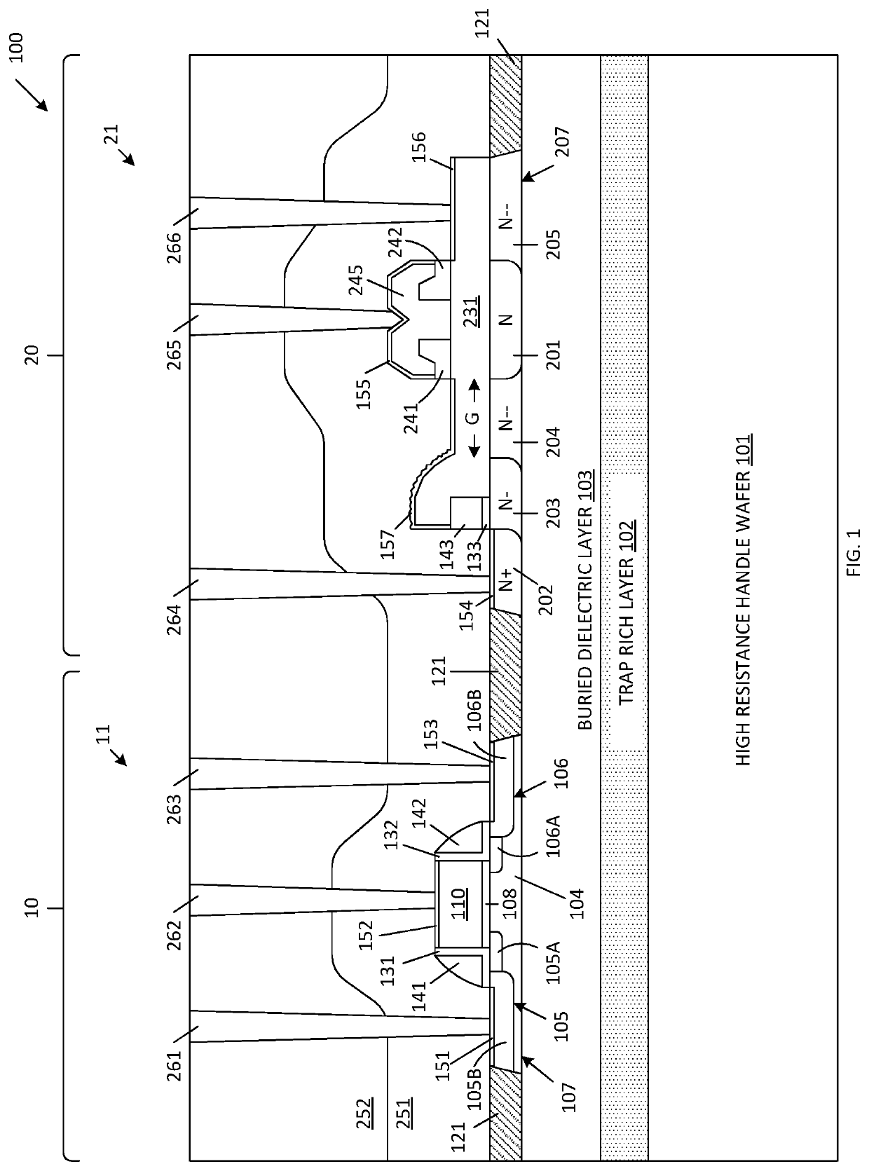
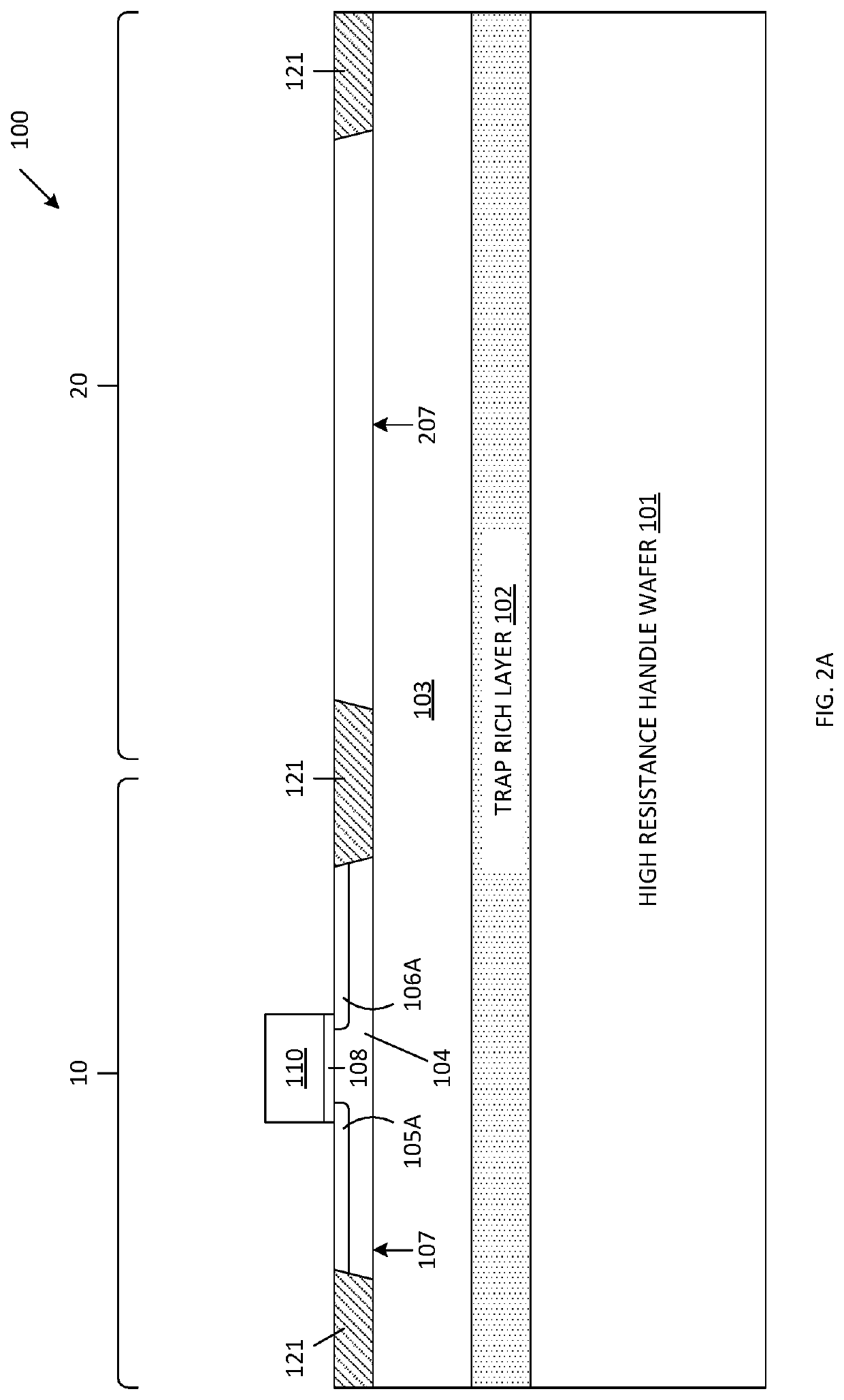
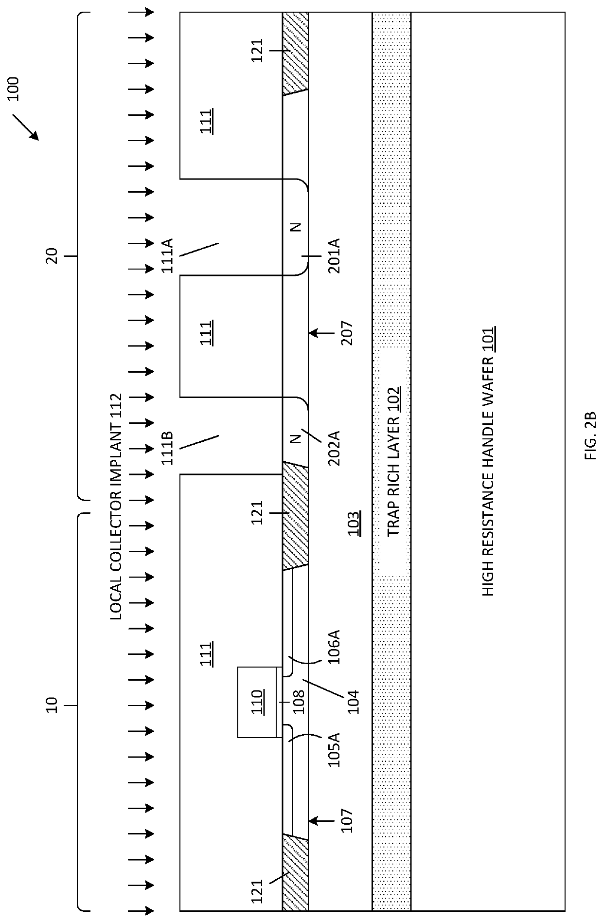
[0023]In general, the present invention provides a method for fabricating SOI CMOS devices and SOI SiGe HBT devices on the same semiconductor wafer. The wafer is processed to include two regions, including a first (SOI CMOS) region that includes a silicon-on-insulator structure for the formation of SOI CMOS transistors, and a second (SOI HBT) region that includes a silicon-on-insulator structure for the formation of SOI HBT devices, such as SOI SiGe HBTs. One or more isolation structures, including shallow trench isolation (STI) structures, separate the SOI CMOS region from the SOI HBT region. In one embodiment, the method is used to fabricate a front end module (FEM) of an RF system on a single wafer, wherein SOI CMOS transistors fabricated in the SOI CMOS region are used to implement RF switches of the FEM, and SOI SiGe HBTs fabricated in the SOI HBT region are used to implement amplifiers (e.g., LNAs and PAs) of the FEM. The present invention will now be described in more detail....


PUM

PropertyMeasurementUnit
series resistanceaaaaaaaaaa
thicknessaaaaaaaaaa
thicknessaaaaaaaaaa

Abstract

A silicon-on-insulator (SOI) CMOS transistor and a SOI heterojunction bipolar transistor (HBT) are fabricated on the same semiconductor substrate. First and second SOI regions are formed over the semiconductor substrate. A SOI CMOS transistor is fabricated in the first SOI region, and a collector region of the SOI HBT is fabricated in the second SOI region. The collector region can be formed by performing a first implant to a local collector region in the second SOI region, and performing a second implant to an extrinsic collector region in the second SOI region, wherein the extrinsic collector region is separated from the local collector region. A SiGe base is formed over the collector region, wherein a dielectric structure separates portions of the SiGe region and the extrinsic collector region. The SOI CMOS transistor and SOI HBT may be used to implement a front end module of an RF system.

Description

FIELD OF THE INVENTION[0001]The present invention relates to an improved process that allows for the fabrication of silicon-on-insulator (SOI) CMOS devices and SOI silicon-germanium (SiGe) heterojunction bipolar transistor (HBT) devices on the same wafer, and structures formed using the same. More specifically, the present invention relates to the fabrication of SOI HBT devices using a process that is largely consistent with a conventional process used to fabricate SOI CMOS devices.RELATED ART[0002]Two components needed in every radio frequency (RF) front-end-module (FEM) include an RF switch and one or more amplifiers. For modern cell phone based FEMs, the technology of choice for implementing RF switches is silicon-on-insulator (SOI) CMOS transistors, due to the excellent performance provided by these transistors in terms of low RF losses (due to the low resistance exhibited by SOI CMOS transistors in the on-state, and the low capacitance exhibited by SOI CMOS transistors in the o...

Claims


Application Information

Patent Timeline
Patent Type & Authority Patents(United States)
IPC IPC(8): H01L21/84H01L29/06H01L29/10H01L29/737H01L27/12H01L29/165H01L27/06H01L21/8249H01L29/66
CPCH01L21/84H01L29/165H01L29/66242H01L29/0692H01L29/1004H01L29/737H01L27/1203H01L29/66272H01L29/7371H01L27/0623H01L21/8249
Inventor PREISLER, EDWARD J.HURWITZ, PAUL D.RACANELLI, MARCOHOWARD, DAVID J.
Owner HARBOR ISLAND DYNAMIC LLC
Why Eureka
Try Eureka