
Light emitting device with an electrostatic discharge (ESD) suppression pattern having first and second conductive particles dispersed in a resin

a light emitting device and suppression pattern technology, applied in the direction of semiconductor devices, basic electric elements, electrical equipment, etc., can solve the problems of lowering the light emitting output of the light emitting device, damaging the active layer in which light is generated, etc., to prevent the damage of the light emitting structure caused by static electricity and improve the dispersibility of the first particle

Active Publication Date: 2020-03-10
SUZHOU LEKIN SEMICON CO LTD
View PDF12 Cites 0 Cited by
  • Summary
  • Abstract
  • Description
  • Claims
  • Application Information

AI Technical Summary

Benefits of technology

[0011]A light emitting device of the present disclosure has the following effects.
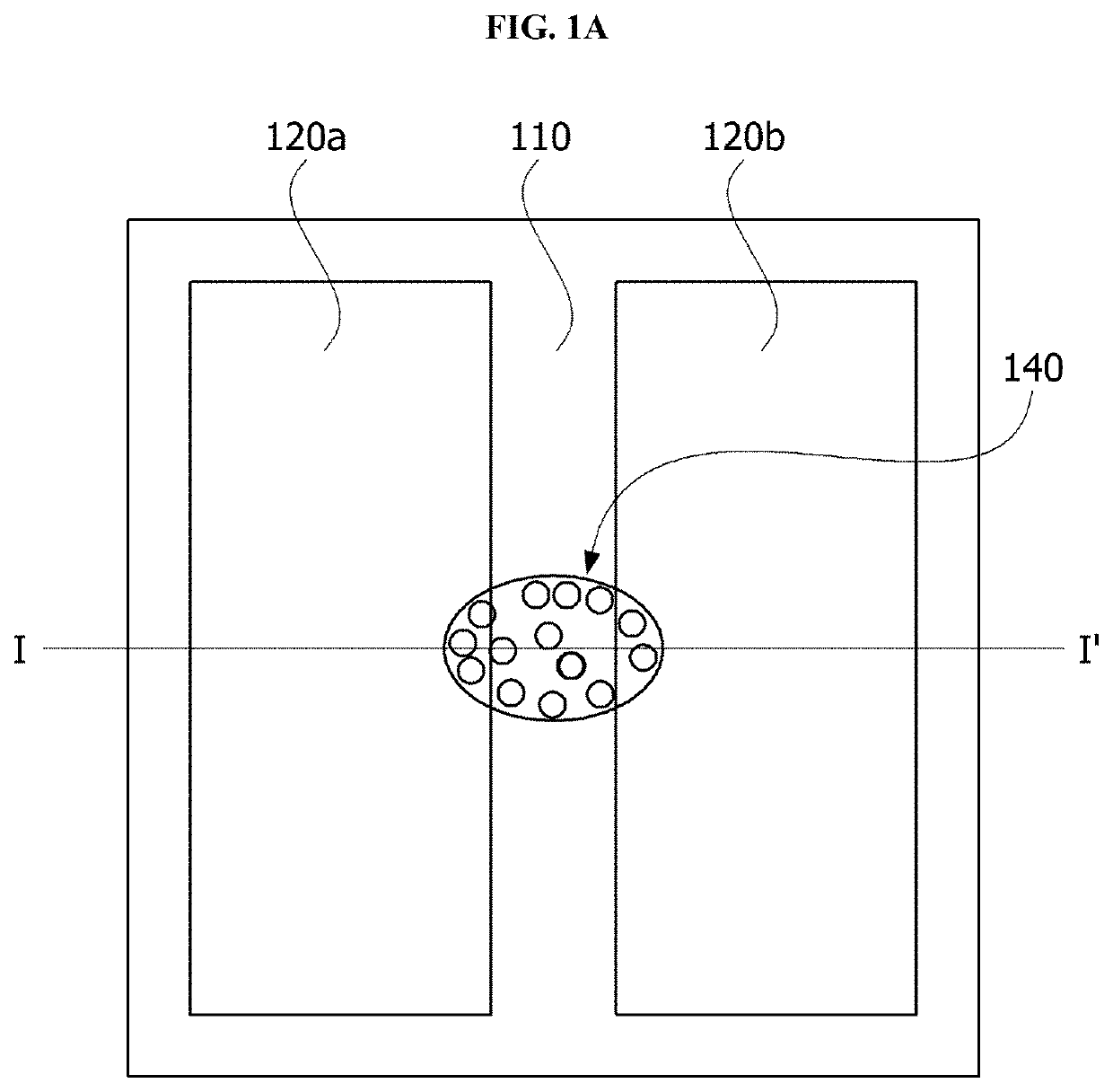
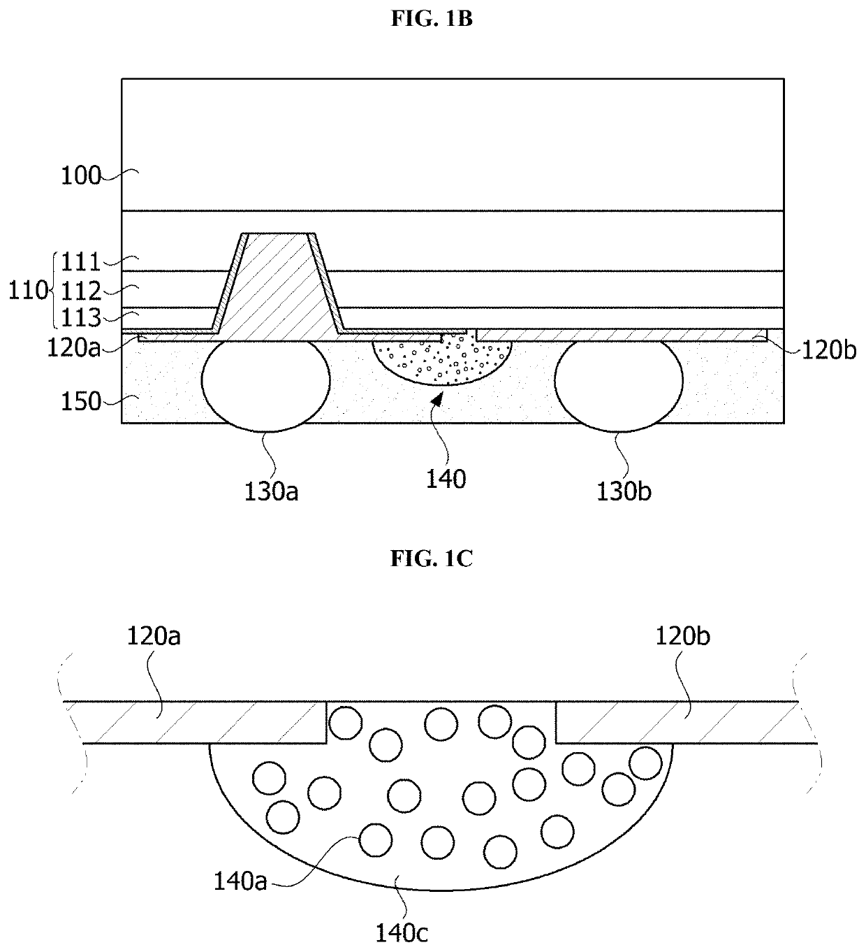
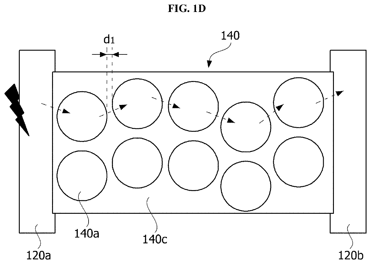
[0012]First, an electrostatic discharge suppression pattern including a resin in which first particles are dispersed is disposed between first and second electrodes and disposed to partially cover the first and second electrodes, and thus the electrostatic discharge suppression pattern functions as an insulator or a conductor based on a threshold voltage thereof. Therefore, when a voltage higher than or equal to the threshold voltage is supplied to the light emitting device, the electrostatic discharge suppression pattern can function as a conductor and thus a current path can be formed between the first and second electrodes. Accordingly, the damage of the light emitting structure caused by static electricity can be prevented.
[0013]Second, in order to improve the dispersibility of the first particles, the threshold voltage of the electrostatic discharge suppression pattern can be adjusted by adjusting an amount of second particles which are further dispersed in the resin or by adjusting diameters of the first particles.

Problems solved by technology

However, when electrostatic discharge (ESD) occurs, a current may flow in a reverse direction, thereby damaging the active layer in which light is generated.
In this case, however, since a process of mounting the device is further added and the device absorbs light emitted from the light emitting device, a problem of lowering the light emitting output of the light emitting device occurs.

Method used


Image

  • Light emitting device with an electrostatic discharge (ESD) suppression pattern having first and second conductive particles dispersed in a resin
  • Light emitting device with an electrostatic discharge (ESD) suppression pattern having first and second conductive particles dispersed in a resin
  • Light emitting device with an electrostatic discharge (ESD) suppression pattern having first and second conductive particles dispersed in a resin

Examples


Embodiment Construction

[0030]While the present disclosure is open to various modifications and alternative forms, specific embodiments thereof are shown by way of example in the drawings and will herein be described in detail. However, it should be understood that there is no intent to limit the present disclosure to the particular forms disclosed, and on the contrary, the present disclosure is to cover all modifications, equivalents, and alternatives falling within the spirit and scope of the present disclosure.

[0031]It should be understood that, although the terms “first,”“second,” etc. may be used herein to describe various elements, these elements are not to be limited by these terms. These terms are only used to distinguish one element from another. For example, a first element could be termed a second element and, similarly, a second element could be termed a first element without departing from the scope of the present disclosure. As used herein, the term “and / or” includes any and all combinations ...


PUM

PropertyMeasurementUnit
distance d1aaaaaaaaaa
thicknessaaaaaaaaaa

Abstract

One embodiment relates to a light emitting device which is free from electrostatic discharge by using an electrostatic discharge suppressing pattern including a resin having particles conductive and dispersed therein, the light emitting device comprising: a light emitting structure including a first conductive semiconductor layer, an active layer, and a second conductive semiconductor layer; a first electrode connected with the first conductive semiconductor layer; a second electrode connected with the second conductive semiconductor layer; and an electrostatic discharge suppressing pattern, which is overlapped with the first electrode and the second electrode, and of which first particles are dispersed in the resin so as to cover a gap between the first electrode and the second electrode.

Description

CROSS-REFERENCE TO RELATED PATENT APPLICATIONS[0001]This application is a U.S. National Stage Application under 35 U.S.C. § 371 of PCT Application No. PCT / KR2016 / 011922, filed Oct. 21, 2016, which claims priority to Korean Patent Application No. 10-2015-0146615, filed Oct. 21, 2015, whose entire disclosures are hereby incorporated by reference.TECHNICAL FIELD[0002]Embodiments of the present disclosure relate to a light emitting device which is free from electrostatic discharge.BACKGROUND ART[0003]A light emitting diode (LED) is one of light emitting elements that emit light when a current is supplied thereto. LEDs can emit light having high efficiency at a low voltage and thus have a high energy saving effect. Recently, a problem with the luminance of LEDs has been significantly addressed, and LEDs are being applied in various devices such as backlight units of liquid crystal display (LCD) devices, electronic sign boards, indicators, home appliances, and the like.[0004]LEDs may have...

Claims


Application Information

Patent Timeline
Patent Type & Authority Patents(United States)
IPC IPC(8): H01L33/36H01L25/16H01L33/44H01L33/62H01L33/48H01L33/38
CPCH01L33/36H01L25/167H01L33/382H01L33/44H01L33/62H01L33/486
Inventor HONG, JUN HEEHWANG, DEOK KIKIM, HOE JUNLIM, WOO SIK
Owner SUZHOU LEKIN SEMICON CO LTD
Learn More