
Patch panel frame for circuit board module

a circuit board module and patch panel technology, applied in the field of structure, can solve the problems of reducing the space available for manipulating cables, time-consuming to change out patch panel components, and wasting time terminating cables, so as to facilitate upgrading and repairing of patch panels

Inactive Publication Date: 2019-09-17
MOLEX INC
View PDF101 Cites 0 Cited by
  • Summary
  • Abstract
  • Description
  • Claims
  • Application Information

AI Technical Summary

Benefits of technology

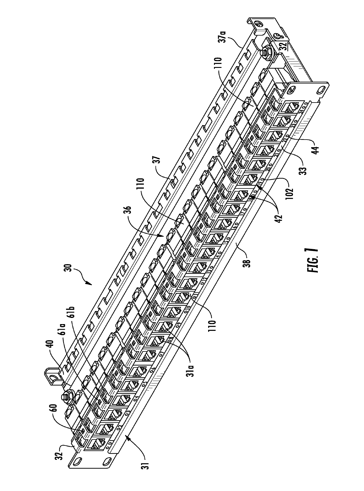
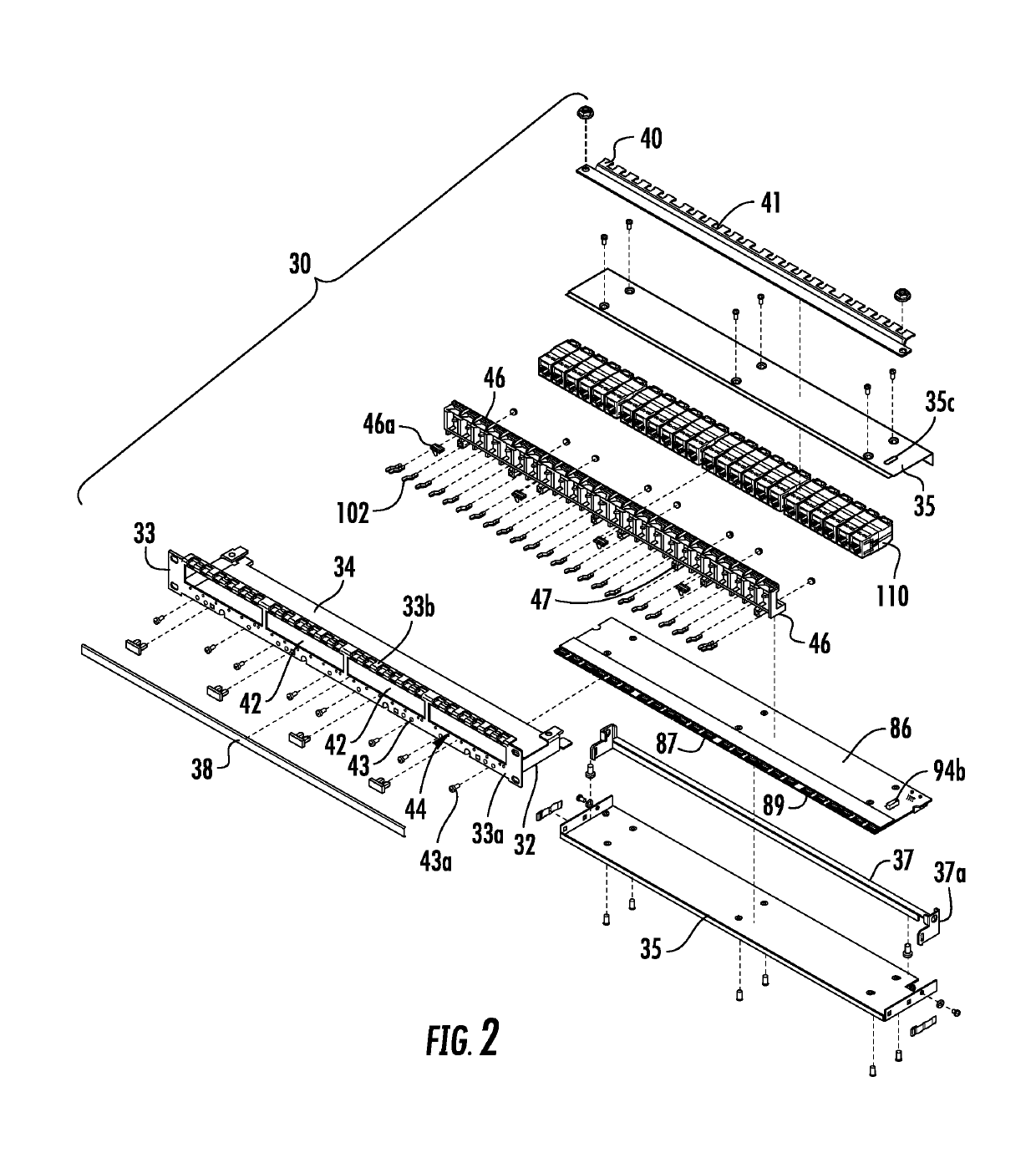
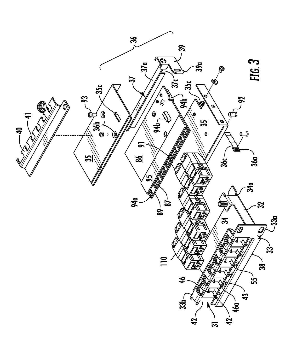
The present patent provides a patch panel assembly with a modular structure and replaceable circuit boards and port jacks that make upgrading and repairing easier. A housing-style connector and a light pipe assembly are also provided. An improved data jack and an electronic module for monitoring patch cord placement and network connectivity are also provided. These features facilitate quicker upgradation and repair of patch panels.

Problems solved by technology

Without this capability, much time and energy would be spent terminating cable that would have to be hard-wired.
The data cables and their associated wires are supported on a frame at the rear of the panel and these cables tend to reduce the space available for manipulation of the cables.
It is very time-consuming to change out patch panel components and the tight clearances associated with them make the changing, or upgrading, process difficult.
Changing or upgrading conventional patch panel assemblies is troublesome as the jacks may be mounted all together, as shown and described in U.S. Pat. No. 8,251,707, issued 28 Aug. 2012 to the assignee of the Present Disclosure, the content of which is hereby incorporated herein in its entirety, in an arrangement upon one side of a first circuit board and termination blocks for the jacks are mounted on the opposite side of the first circuit board.
This takes a longer time than desirable and the negative effect of structures such as these are that it becomes close to impossible to do panel upgrades efficiently as all the panel components must be removed to access a single jack or other components.
Additionally, with such a structure, a user must purchase all the components necessary for all 24 ports of the patch panel and cannot simply start with a few ports and subsequently increase the capability of the patch panel.
This can weaken already thin budgets for an enterprise that seeks to increase its IT capability as it grows.
The structures shown in the '707 patent are not modular and cannot be replaced in smaller, discrete groups.
That is one disadvantage to a conventional patch panel assembly.
Another disadvantage to such conventional patch panel structures is, as noted above, where the data jacks and termination blocks are mounted directly to a first circuit board or a monolithic circuit board assembly, care must be taken and specialized tools may need to be used to properly effect the termination of the wires of the data cables in a manner not to unduly transfer termination forces to the first circuit board.
Similarly, because the jacks are affixed to the first circuit board, these conventional patch panel systems do not have any “pluggable” aspect to their jacks, where an installer can merely insert each jack individually into a housing, after terminating the cable wires to it, in order to repair, replace or upgrade the jack.
Failure of the components associated with one or more panel ports requires removal of the entire circuit board and usually replacement of it, as well.
This is expensive when not all of the ports in the panel have failed or need attention.
The known patch panel assemblies described above do not permit individual port repair or replacement insofar as the circuit boards and the electronic components mounted thereon are concerned.

Method used


Image

  • Patch panel frame for circuit board module
  • Patch panel frame for circuit board module
  • Patch panel frame for circuit board module

Examples


Embodiment Construction

[0055]While the Present Disclosure may be susceptible to embodiment in different forms, there is shown in the Figures, and will be described herein in detail, specific embodiments, with the understanding that the Present Disclosure is to be considered an exemplification of the principles of the Present Disclosure, and is not intended to limit the Present Disclosure to that as illustrated.

[0056]As such, references to a feature or aspect are intended to describe a feature or aspect of an example of the Present Disclosure, not to imply that every embodiment thereof must have the described feature or aspect. Furthermore, it should be noted that the description illustrates a number of features. While certain features have been combined together to illustrate potential system designs, those features may also be used in other combinations not expressly disclosed. Thus, the depicted combinations are not intended to be limiting, unless otherwise noted.

[0057]In the embodiments illustrated in ...


PUM


Abstract

An improved patch panel assembly includes a frame and faceplate that mate with a housing, and the housing defines a plurality of individual communication ports. The housing is mounted to the patch panel frame and includes jack openings that accommodate data jacks and circuit board openings that accommodate mating blades of circuit boards. The two sets of openings are separated on the housing by an intervening spacing and interposer terminal sets are provided to electrically interconnect the jacks with circuits on the circuit boards. The patch panel housings may be formed in discrete groupings so that, if desired, the patch panels may have ports that are grouped together by bandwidth, storage capability and the like. Inasmuch as the housings are mounted to the patch panel frames, the jacks and the circuit boards can be easily and individually replaced, repaired or upgraded with similar components without requiring disassembly of the patch panel.

Description

RELATED CASES[0001]This application claims priority to U.S. Provisional Application No. 62 / 033,965, filed Aug. 6, 2014, which is incorporated herein by reference in its entirety.BACKGROUND OF THE PRESENT DISCLOSURE[0002]The Present Disclosure relates, generally, to structures utilized in data transmission networks, and, more particularly, to network panel assemblies, jacks for such assemblies, housings for holding such jacks in place within such assemblies, and light pipe arrangements for such assemblies all having improved structures that facilitate quick and reliable upgrading and assembly of data transmission networks.[0003]Data transmission networks are widely used in business operations, including financial, retail, manufacturing, medical, education and engineering sectors. They typically are comprised of a central server or computer storage unit that is linked, or networked, to a plurality of end user devices. Such end user devices include any device that transmits or receives...

Claims


Application Information

Patent Timeline
Patent Type & Authority Patents(United States)
IPC IPC(8): H01R13/514H01R13/627H01R13/66H01R13/717H01R13/74H01R24/64H01R13/518H01R25/00H01R107/00
CPCH01R13/74H01R13/518H01R13/514H01R13/665H01R13/7175H01R25/006H01R13/6275H01R24/64H01R2107/00
Inventor BAINES, ELLIOT A.SCHNEIDER, GENEFREDERIKSEN, BJARNERIVERS, PHILIPPANELLA, AUGUSTO
Owner MOLEX INC
Learn More