Wide dynamic range image sensor pixel cell

Active Publication Date: 2019-08-27
SMARTSENS TECH (HK) CO LTD
View PDF8 Cites 37 Cited by
  • Summary
  • Abstract
  • Description
  • Claims
  • Application Information

AI Technical Summary

Benefits of technology

This patent describes a new pixel cell and readout method for a camera that can capture high-quality images in low-light conditions. The pixel cell has two photodiodes: one for bright light conditions and one for low-light conditions. The smaller of the two photodiodes is exposed to incident light in a chopped manner while the larger photodiode is exposed at a constant manner. The pixel cell also uses dual conversion gain and shuttered exposure to enhance signal dynamic range. Additionally, a unique construction of the pixel cell allows for the option to read out the low-light photodiode in either rolling shutter or global shutter mode. The pixel cell is designed to be able to capture both high-light and dark-shadow scenes while maintaining high image quality. Overall, this patent is about improving image quality in the dark and enhancing dynamic range through special construction of the pixel cell.

Problems solved by technology

However, miniaturization has come with the loss of pixel photosensitivity and dynamic range which require new approaches in order to mitigate.
With the decreased pixel size, the total light absorption depth within the substrate becomes insufficient for some light, especially long-wavelength light.
This becomes a particular problem for image sensors using backside illumination (BSI) technology wherein the image light is incident upon the backside of the sensor substrate.
In BSI technology the sensor Silicon substrate may be only two microns (micrometers) thick which is adequate to absorb blue light but very inadequate to absorb red light which may require ten microns of thickness to be fully absorbed.
A potential disadvantage of rolling shutter readout mode is spatial distortion which results from the above.
Another disadvantage is that different regions of the exposed image will not be precisely correlated in time and appear as a distortion in the image.
However it carries risk of spatial distortion especially when imaging relatively large, fast moving objects.
This effect is commonly known as “flicker” and may limit imaging in applications such as LED automotive lights, road signs, and traffic signs as well as in security and surveillance.
Flicker avoidance is more challenging when employing high dynamic range (HDR) imaging systems to capture scenes with some very bright regions and some very dark regions while maintaining high image quality in low light conditions.
However, this approach has fundamental issues associated with the different exposure timings for long and short exposures, which can generate artifacts against moving objects or time-varying light sources like pulsed LEDs.

Method used


Image

  • Wide dynamic range image sensor pixel cell
  • Wide dynamic range image sensor pixel cell
  • Wide dynamic range image sensor pixel cell

Examples


first embodiment

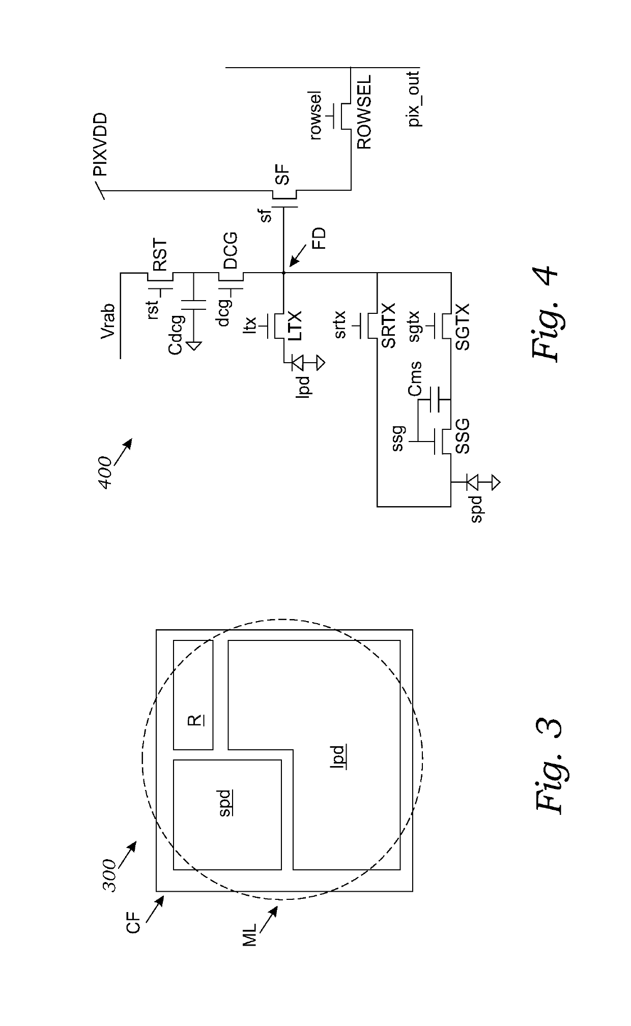
[0039]In summary, as a result of the described circuit diagram of FIG. 4 and the described control signal timing diagram of the invention four separate signals and their respective reference levels are generated and readout for each pixel cell leading to a widening of the dynamic range of the resultant signal representing the illumination incident upon the dual photodiode pixel. An advantage of the invented pixel cell is that the dual conversion gain components are shared by the large and small photodiodes rather than constrained to have separate dual conversion gain components assigned to each photodiode. The read out methods illustrated in FIG. 5 would be more commonly be used in a row by row rolling shutter readout method for both the large and small photodiodes but the presence of storage elements Cms and SGTX it is to be understood that in another embodiment of the invention the small photodiode may be exposed and read out in a global shutter mode while the large photodiode is ...

second embodiment

[0041]FIG. 6 is an electrical schematic diagram of a pixel cell in accordance with the invention. FIG. 6 illustrates pixel cell 600 comprising the same signal dynamic range enhancing features shown in FIG. 4 but with an alternative connection scheme. The pixel cell electrical schematic illustrated in FIG. 6 is the same as the one shown in FIG. 4 with the exception that transistor SRTX connects small photodiode spd to node D, the node between dynamic enhancement capacitor Cdcg and capacitor control transistor DCG, rather than at the node between transistor DCG and floating drain FD. A control timing diagram similar to FIG. 5 can be used to read out imaging signals providing enhanced dynamic range.

[0042]Further embodiments of the invention may be realized by the choice of fabrication method for capacitors Cdcg and Cms. These capacitors may be fabricated as metal-insulator-metal (MIM) capacitors, metal-oxide-metal (MOM) capacitors or metal-oxide-silicon (MOS) capacitors. There are also...


PUM


Abstract

A pixel cell has a large and small photodiode, transfer transistors, a reset transistor, a dynamic range enhancement capacitor, a capacitor control transistor, a storage capacitor, a storage capacitor control transistor, an amplifier transistor in a source follower configuration and a rolling shutter row select transistor and a readout circuit block. The small and large photodiodes are exposed simultaneously, the large photodiode having a constant exposure while the small photodiode has a chopped exposure and charge transfer to a storage capacitor.

Description

BACKGROUND OF THE INVENTIONField of the Invention[0001]This invention relates generally to image sensors, and more particularly to CMOS image sensors. The present invention provides a pixel cell design and method for obtaining wide dynamic range images. An image sensor comprising the invented pixel design and method may be incorporated within a digital camera.Description of Related Art[0002]An image capture device includes an image sensor and an imaging lens. The imaging lens focuses light onto the image sensor to form an image, and the image sensor converts the light into electrical signals. The electric signals are output from the image capture device to other components of a host electronic system. The image capture device and the other components of a host electronic system form an imaging system. Image sensors have become ubiquitous and may be found in a variety of electronic systems, for example a mobile device, a digital camera, a medical device, or a computer.[0003]A typical...

Claims


Application Information

Patent Timeline
IPC IPC(8): H04N5/355H04N5/3745
CPCH04N25/59H04N25/78H04N25/585H04N25/771H04N25/778H04N25/75
Inventor XU, CHENMO, YAOWUSHAO, ZEXUZHANG, ZHENGMINMA, WEIJIAN
Owner SMARTSENS TECH (HK) CO LTD
Why Eureka
Try Eureka