
Electromagnetic bandgap structure and method for manufacturing the same

a technology of electromagnetic bandgap and bandgap, which is applied in the direction of cross-talk/noise/interference reduction, waveguide type devices, printed element electric connection formation, etc., can solve the problems of ssn, negative influence of rf circuit, and degraded power quality, so as to suppress simultaneous switching noise of broadband

Inactive Publication Date: 2019-03-19
ELECTRONICS & TELECOMM RES INST
View PDF56 Cites 0 Cited by
  • Summary
  • Abstract
  • Description
  • Claims
  • Application Information

AI Technical Summary

Benefits of technology

[0013]Accordingly, the present invention has been made keeping in mind the above problems occurring in the prior art, and an object of the present invention is to provide an electromagnetic bandgap structure, which satisfies the characteristics of a low resonance suppression start frequency and broadband resonance suppression so as to suppress broadband simultaneous switching noise on a power plane and a ground plane.
[0015]A further object of the present invention is to stably operate a system by cancelling power-ground noise in a broadband range.
[0016]Yet another object of the present invention is to provide an electromagnetic bandgap structure, which can be applied to a multimedia device in which broadband SSN occurs by overcoming the limitation of a conventional mushroom-like electromagnetic bandgap structure, the noise cancellation frequency band of which is narrow.

Problems solved by technology

Digital circuits operating in such a high frequency band cause simultaneous switching noise (SSN) extending to a broadband range.
Therefore, SSN occurring in a digital circuit consequently leads to the power-ground plane through a via or the like connected to the power-ground plane, and moves along the power-ground plane due to the TEM resonance mode formed on the power-ground plane, so that SSN is propagated to other circuits or is radiated from the end of a printed circuit board, thus negatively influencing RF circuits.
For these reasons, power quality is degraded or a power margin is decreased due to the malfunction of analog circuits or the like.
Further, such SSN causes problems in that it deteriorates signal quality by distorting the waveform of digital signals and also deteriorates communication performance due to the noise induced in RF circuits.
However, a problem may arise in that a decoupling capacitor must be populated on a PCB and costs are increased and in that, when a frequency is increased, inherent parasitic inductance of the decoupling capacitor causes another parallel resonant frequency.
Further, there is a disadvantage in that noise having a GHz frequency component, which is problematic in a fast digital system, cannot be suppressed.
However, the method for suppressing noise using the dielectric substrate is of limited usefulness due to the problem of requiring an additional manufacturing process and thus incurring additional expenses.
However, since the sizes of multimedia devices are reduced, the size of a PCB is also reduced, and thus there is a limitation on the extent to which the size of an EBG structure can be increased.
In practice, the size of an EBG structure is decreased instead, thus resulting in an increase in the resonant frequency occurring between a power plane and a ground plane.

Method used


Image

  • Electromagnetic bandgap structure and method for manufacturing the same
  • Electromagnetic bandgap structure and method for manufacturing the same
  • Electromagnetic bandgap structure and method for manufacturing the same

Examples


Embodiment Construction

[0042]The present invention may be variously changed and may have various embodiments, and specific embodiments will be described in detail below with reference to the attached drawings.

[0043]However, it should be understood that those embodiments are not intended to limit the present invention to specific disclosure forms and they include all changes, equivalents or modifications included in the spirit and scope of the present invention.

[0044]The terms used in the present specification are merely used to describe specific embodiments and are not intended to limit the present invention. A singular expression includes a plural expression unless a description to the contrary is specifically pointed out in context. In the present specification, it should be understood that the terms such as “include” or “have” are merely intended to indicate that features, numbers, steps, operations, components, parts, or combinations thereof are present, and are not intended to exclude a possibility t...


PUM


Abstract

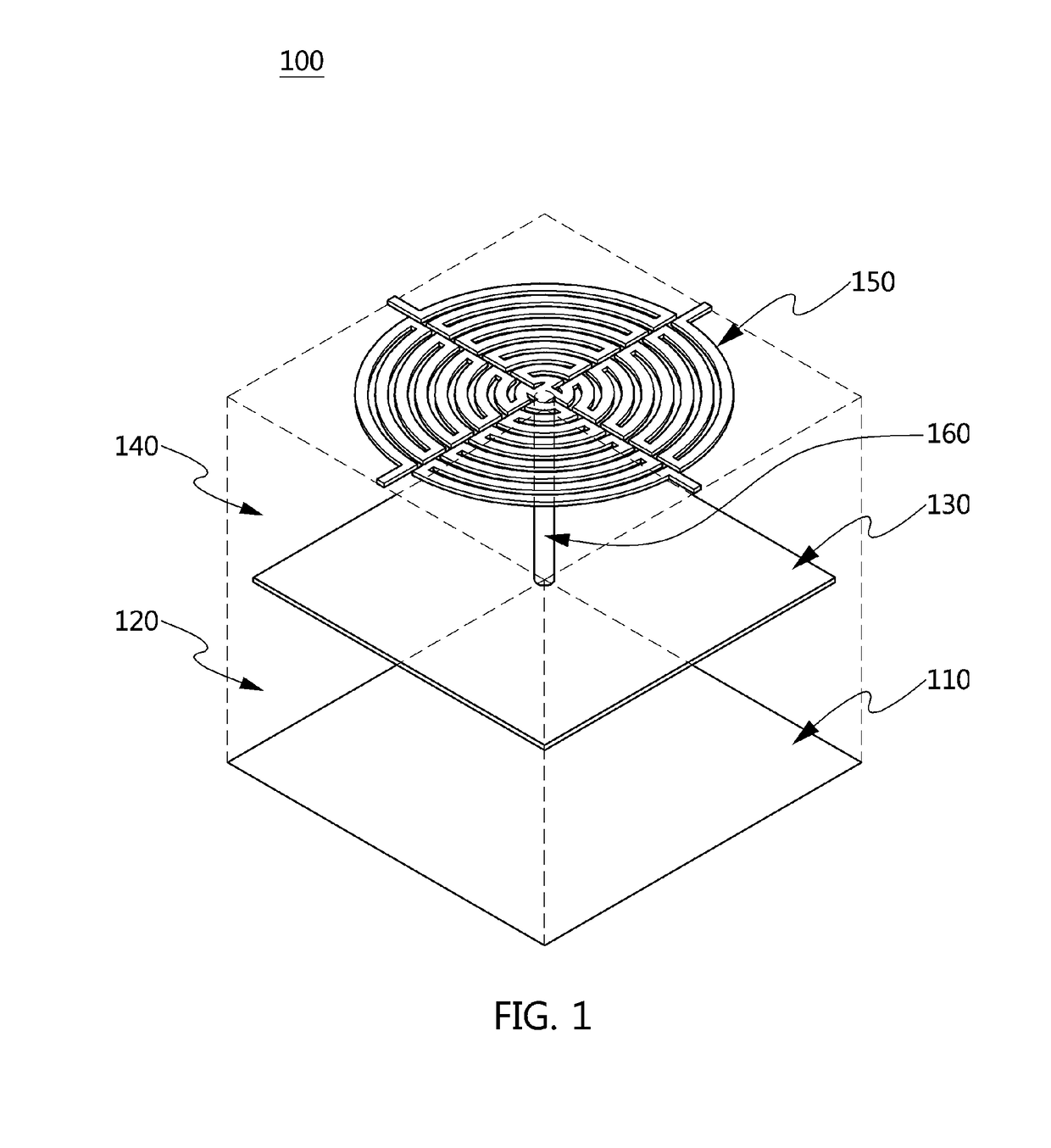
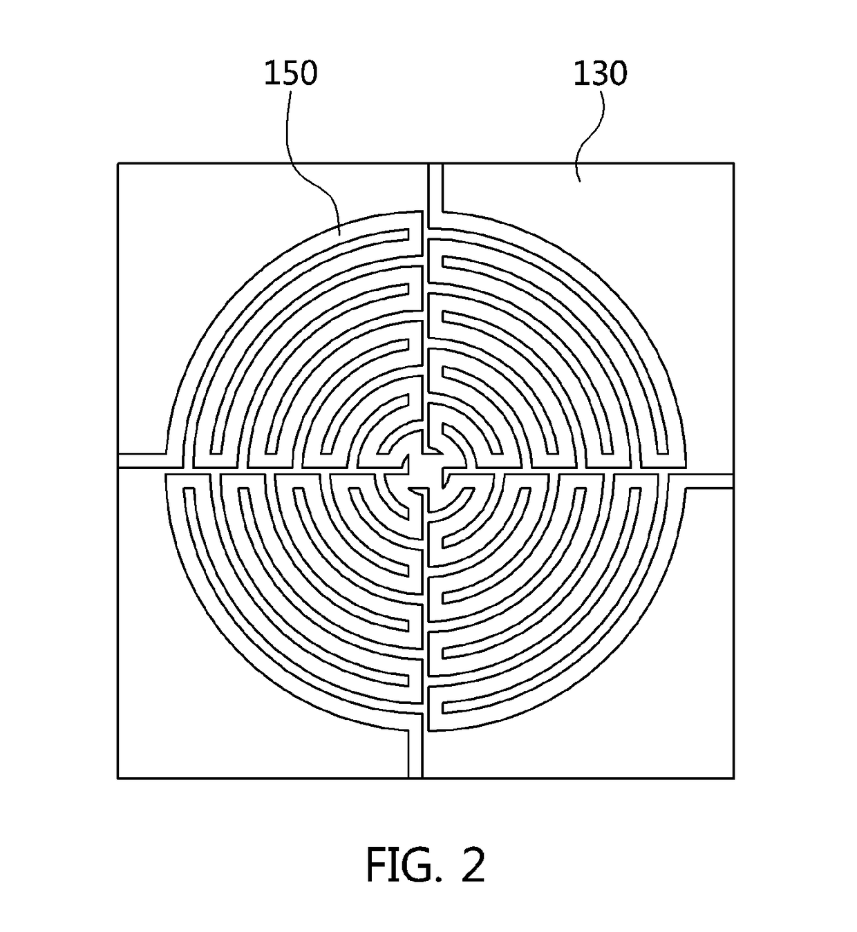
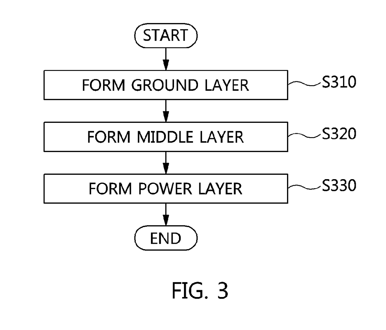
Disclosed are an electromagnetic bandgap structure and a method for manufacturing the same. The electromagnetic bandgap structure includes a ground layer, a middle layer configured to include one or more patches, and to face the ground layer with a first dielectric layer interposed between the middle layer and the ground layer, wherein the first dielectric layer is stacked on a top of the ground layer, and a power layer configured to face the middle layer with a second dielectric layer interposed between the power layer and the middle layer, wherein the second dielectric layer is stacked on a top of the patches, wherein the patches and the power layer are electrically connected to each other through a via.

Description

CROSS REFERENCE TO RELATED APPLICATION[0001]This application claims the benefit of Korean Patent Application No. 10-2016-0114330, filed Sep. 6, 2016, which is hereby incorporated by reference in its entirety into this application.BACKGROUND OF THE INVENTION1. Technical Field[0002]The present invention relates generally to an Electromagnetic Bandgap (EBG) structure and, more particularly, to an electromagnetic bandgap structure which blocks the transmission of broadband noise present between a power plane and a ground plane on a printed circuit board on which mixed signals are used together.2. Description of the Related Art[0003]Recently, the current trend of data communication equipment including multimedia devices is towards the implementation of small size and light weight and the integration of circuits as handheld functions are required. For this trend, designs for the small-size implementation and integration of embedded circuits have been realized, and digital circuits and ana...

Claims


Application Information

Patent Timeline
Patent Type & Authority Patents(United States)
IPC IPC(8): H05K1/00H05K1/11H05K1/02H05K3/40H05K3/46H05K1/16
CPCH05K1/0236H05K1/115H05K3/4644H05K3/4038H05K2201/09263H05K1/165H01P1/2005H01Q15/006H01Q15/008H05K2201/09309
Inventor LEE, HONGYEAL
Owner ELECTRONICS & TELECOMM RES INST
Learn More