
Process for producing polycrystalline silicon

a polycrystalline silicon and processing technology, applied in silicon compounds, packaging goods types, transportation and packaging, etc., can solve the problems of not being very practicable, difficult to handle, and increasing the risk of bag damage proportionally with the mass of the chunk, so as to achieve less expensive and economic viability.

Active Publication Date: 2019-02-12
WACKER CHEM GMBH
View PDF12 Cites 0 Cited by
  • Summary
  • Abstract
  • Description
  • Claims
  • Application Information

AI Technical Summary

Benefits of technology

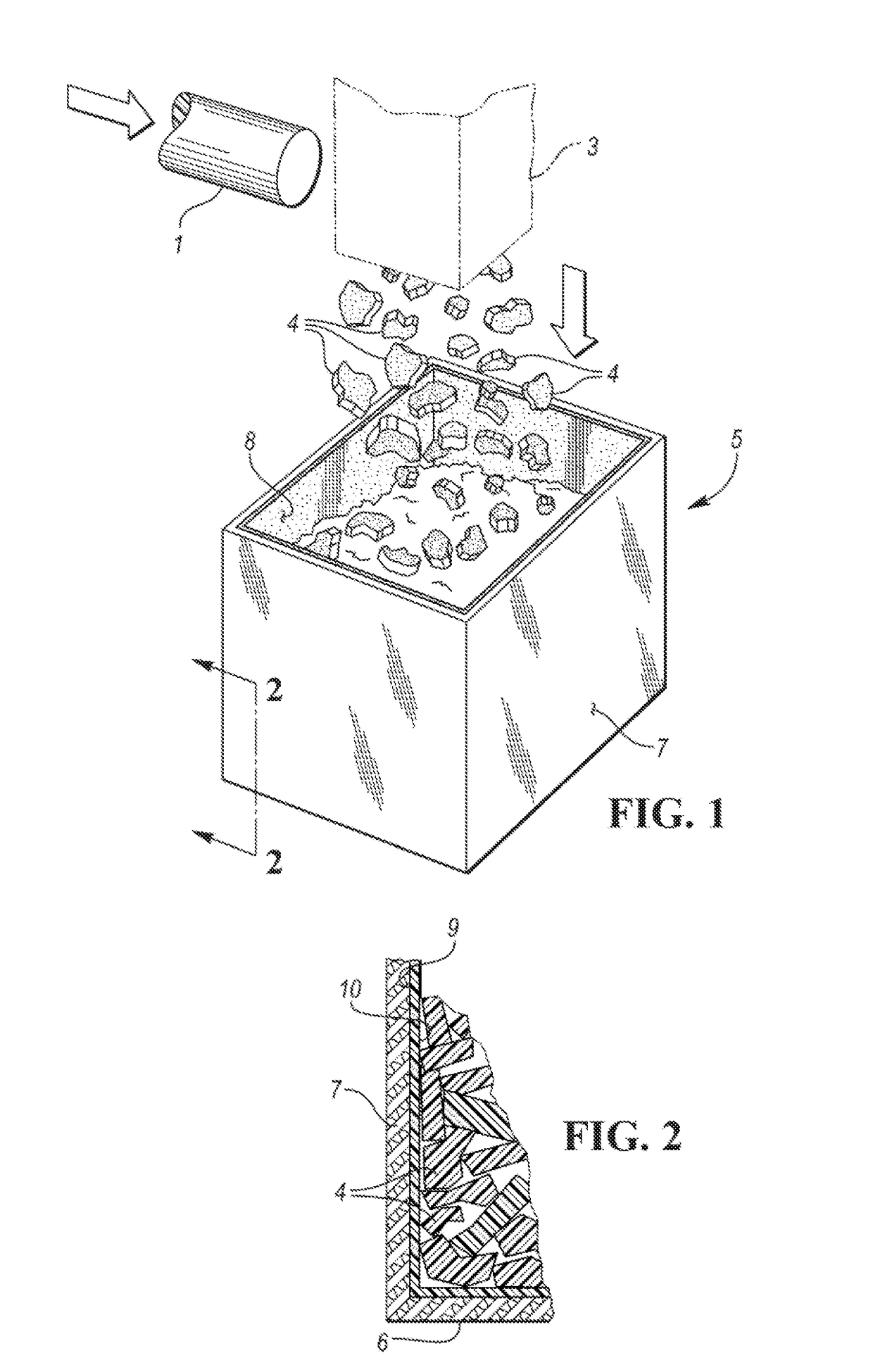
The invention describes a process for making polycrystalline silicon more efficiently and at a lower cost. This is achieved by creating polycrystalline silicon rods and then breaking them into smaller chunks. These chunks are then packed into a cardboard container, which has been coated with plastic on the inside surface to prevent any contamination. This process makes the production of polycrystalline silicon more economical and accessible to a wider range of applications.

Problems solved by technology

The last processing step is always packing in plastic bags, but is problematic because of the fact that chunk polysilicon is a sharp-edged, non-free-flowing bulk material which can penetrate the plastic bag in the course of filling or in the worst case even completely destroy it.
However, this applies only to small or light chunks.
It has been found that the risk of bag damage increases proportionally with the chunk mass.
One conceivable way in principle of reducing the puncture rate by strengthening the bag film has not been found to be very practicable, especially since such a less pliable film would be difficult to handle.
The packing machines being used are not designed for films having a thickness greater than 350 μm.
Moreover, it would take longer to weld such thick bags, which reduces the throughput.
Such puncturing of the bag can occur not just during the packing operation but also in the course of transport to the customer.
Chunks protruding from the bag packing can be unacceptably contaminated directly by surrounding materials, and chunks inside as a result of inflow of ambient air.
This problem is also manifested in the case of so-called double bags, in which the polysilicon is filled into a first bag and this first bag is subsequently introduced into a second bag.

Method used


Image

  • Process for producing polycrystalline silicon

Examples


Embodiment Construction

[0022]The polycrystalline silicon is preferably deposited on heated thin silicon rods, using a silicon-containing component and hydrogen as reaction gas (Siemens process). Preferably, the silicon-containing component is a chlorosilane, more preferably trichlorosilane. The deposition is effected according to the prior art, reference being made, for example, to WO 2009 / 047107 A2.

[0023]After the deposition, the polycrystalline silicon rods are comminuted. Preferably, there is first a preliminary comminution of the polysilicon rods. For this purpose, a hammer made from a low-abrasion material, for example cemented carbide, is used. The preliminary comminution is effected on a workbench having a surface that preferably consists of wear-resistant plastic or of silicon.

[0024]This is followed by comminution of the pre-comminuted polysilicon to the desired target size of chunk size 0, 1, 2, 3, 4 or 5. The chunk size is defined as the longest distance between two points on the surface of a si...


PUM

PropertyMeasurementUnit
thicknessaaaaaaaaaa
thicknessaaaaaaaaaa
thicknessaaaaaaaaaa

Abstract

Polycrystalline silicon chunks are packed for further processing and / or for shipment with minimal contamination by introducing the chunks into a cardboard container lined with a non-contaminating plastic. The process is economical, avoids the problems associated with packaging in plastic bags, and provides far less contamination and spillage during transport.

Description

CROSS REFERENCE TO RELATED APPLICATIONS[0001]This application is the U.S. National Phase of PCT Appln. No. PCT / EP2015 / 054156 filed Feb. 27, 2015, which claims priority to German Application No. 10 2014 203 814.6 filed Mar. 3, 2014, the disclosures of which are incorporated in their entirety by reference herein.BACKGROUND OF THE INVENTION[0002]1. Field of the Invention[0003]The invention relates to a process for producing polycrystalline silicon.[0004]2. Description of the Related Art[0005]Polycrystalline silicon (polysilicon) is predominantly deposited on thin rods from halosilanes such as trichlorosilane by means of the Siemens process, which gives polycrystalline silicon rods, which are then comminuted into polycrystalline silicon chunks. After the comminution into chunks, it is customary to classify these into particular size classes. After sorting and classification, the chunks are dosed to a particular weight and packed in a plastic bag. A corresponding method for sorting, clas...

Claims


Application Information

Patent Timeline
Patent Type & Authority Patents(United States)
IPC IPC(8): B65D5/56C01B33/035B65B1/00C01B33/021B65B1/04B65B63/00
CPCC01B33/021B65B1/00C01B33/035B65B63/00B65D5/563B65B1/04
Inventor VIETZ, MATTHIAS
Owner WACKER CHEM GMBH
Learn More