Microstrip isolation structure for reducing crosstalk
a technology of isolation structure and microstrip, applied in the field of microstrip structure, can solve problems such as not being practical, and achieve the effects of reducing mutual inductance, effective confining magnetic field and depressing, and extremely low coupling with the conventional transmission lin
- Summary
- Abstract
- Description
- Claims
- Application Information
AI Technical Summary
Benefits of technology
Problems solved by technology
Method used
Image
Examples
first embodiment
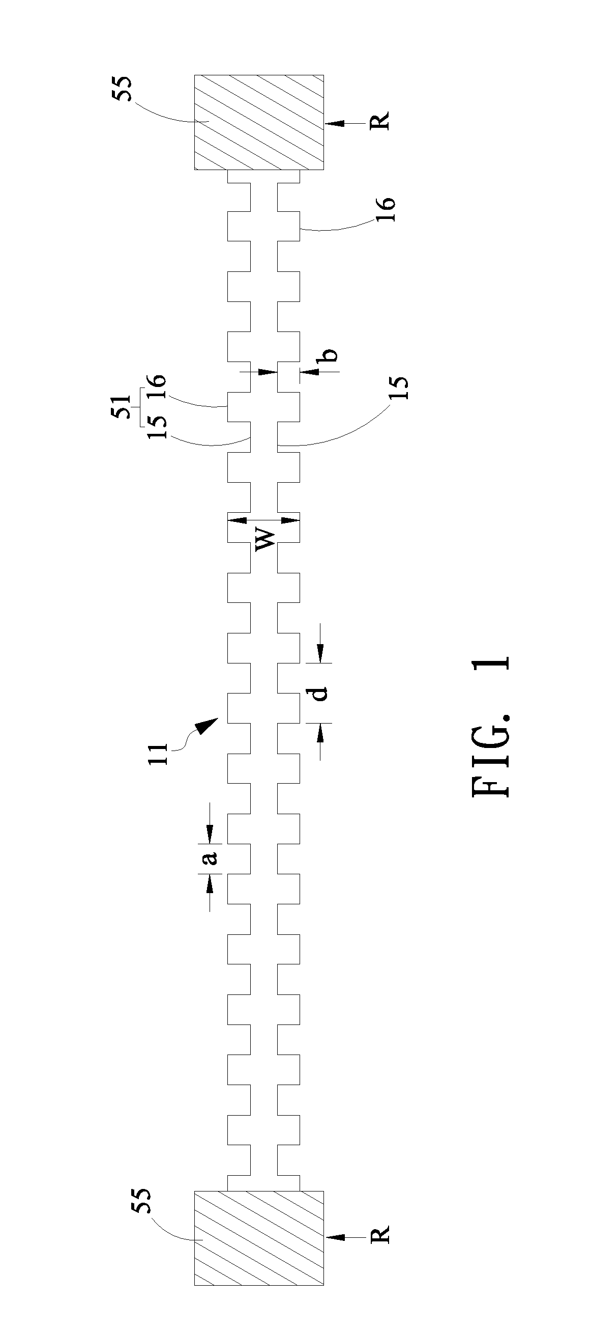
[0036]The present invention provides a microstrip isolation structure for reducing a crosstalk effect. In a first embodiment shown in FIG. 1, the microstrip isolation structure comprises a microstrip line 11 and two resistors 55. The microstrip line 11 has a plurality of indentation structures 51 with periodic arrangement. One resistor 55 is connected to one end of the microstrip line 11 and the other resistor 55 is connected to the other end of the microstrip line 11, wherein the two resistors 55 are grounded and are impedance matched with the microstrip line 11.
[0037]The plurality of indentation structures 51 are periodically formed at two lateral sides of the microstrip line 11 in a subwavelength configuration. In the present embodiment, the plurality of indentation structures are configured by a plurality of rectangle recesses 15 and a plurality of rectangle projections 16 alternately connected to each other. On the microstrip line 11 having subwavelength configuration, an openi...
second embodiment
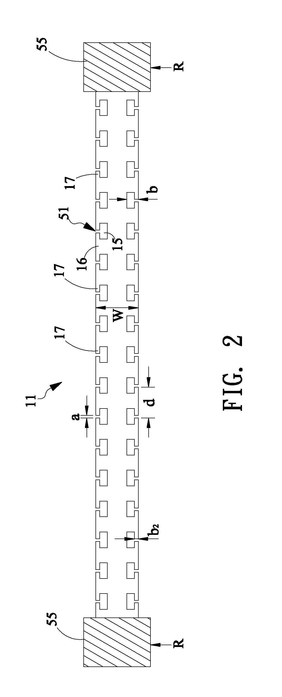
[0038]microstrip isolation structure for reducing crosstalk is shown in FIG. 2, in which the indentation structures 51 formed at two lateral sides of the microstrip isolation structure has bi-directional extension parts. In the present embodiment, the microstrip isolation structure comprises a microstrip line 11 and two resistors 55. The microstrip line 11 has a plurality of indentation structures 51 with periodic arrangement. One end of the microstrip line 11 is connected to one resistor 55 while the other end of the microstrip line 11 is connected to the other resistor 55. The another ends of two resistors 55 are grounded and are impedance matched with the microstrip line 11. The plurality of indentation structures 51 are formed at two corresponding lateral sides of the microstrip line 11 in a subwavelength configuration.
[0039]The indentation structures 51 are configured by a plurality of rectangle recesses 15 and a plurality of rectangle projections 16 alternately connected to ea...
third embodiment
[0041]the microstrip isolation structure having comb structure is illustrated as FIG. 4, wherein the microstrip isolation structure comprises a microstrip line 11 and two resistors 55. The microstrip line 11 comprises a plurality of indentation structures 51 wherein one end of the microstrip line 11 is connected to one resistor 55 while the other end of the microstrip line 11 is connected to the other resistor 55. The two resistors 55 are grounded and are impedance matched with the microstrip line 11. The plurality of indentation structures 51 are periodically formed at two corresponding lateral sides of the microstrip line 11 in a subwavelength configuration.
[0042]Each indentation structure 51 has a recess 19 and a Z-shaped projection 20 connected to the recess 19, wherein each Z-shaped projection 20 further comprises a first extension part 17 connected to the projection body 200, and a second extension part 18 connected to a middle section of the projection body 200, wherein the f...
PUM
 Abstract
Description
Claims
Application Information
 - R&D
- Intellectual Property
- Life Sciences
- Materials
- Tech Scout
- Unparalleled Data Quality
- Higher Quality Content
- 60% Fewer Hallucinations
Browse by: Latest US Patents, China's latest patents, Technical Efficacy Thesaurus, Application Domain, Technology Topic, Popular Technical Reports.
© 2025 PatSnap. All rights reserved.Legal|Privacy policy|Modern Slavery Act Transparency Statement|Sitemap|About US| Contact US: help@patsnap.com


