Surface potential sensor and copying machine
a surface potential sensor and sensor technology, applied in the field of surface potential sensors and copying machines, can solve the problems of deterioration in printing quality, high manufacturing cost, and difficulty in miniaturizing the surface potential sensor, and achieve the effects of low manufacturing cost, small size of surface potential sensor, and low manufacturing cos
- Summary
- Abstract
- Description
- Claims
- Application Information
AI Technical Summary
Benefits of technology
Problems solved by technology
Method used
Image
Examples
first embodiment
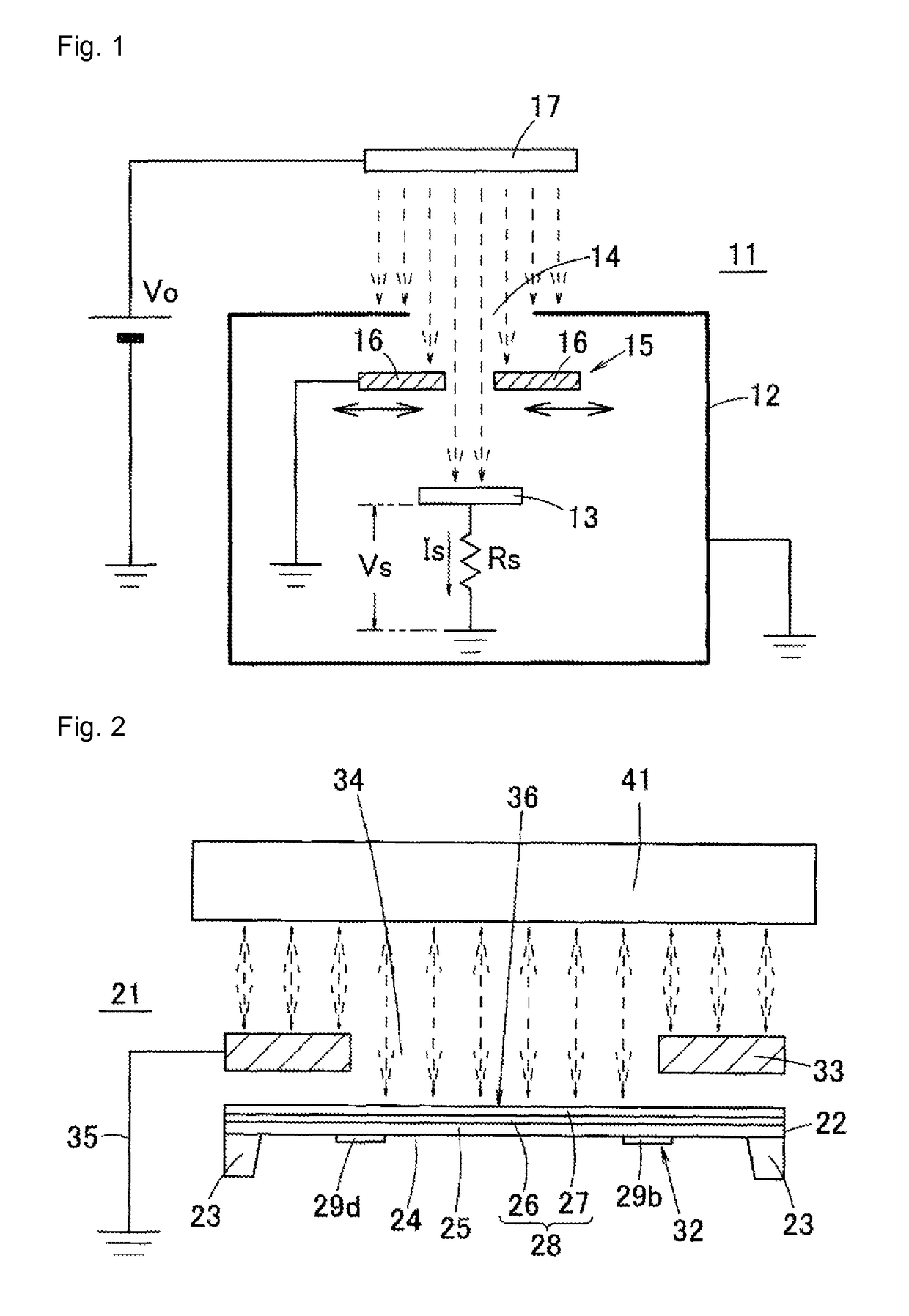
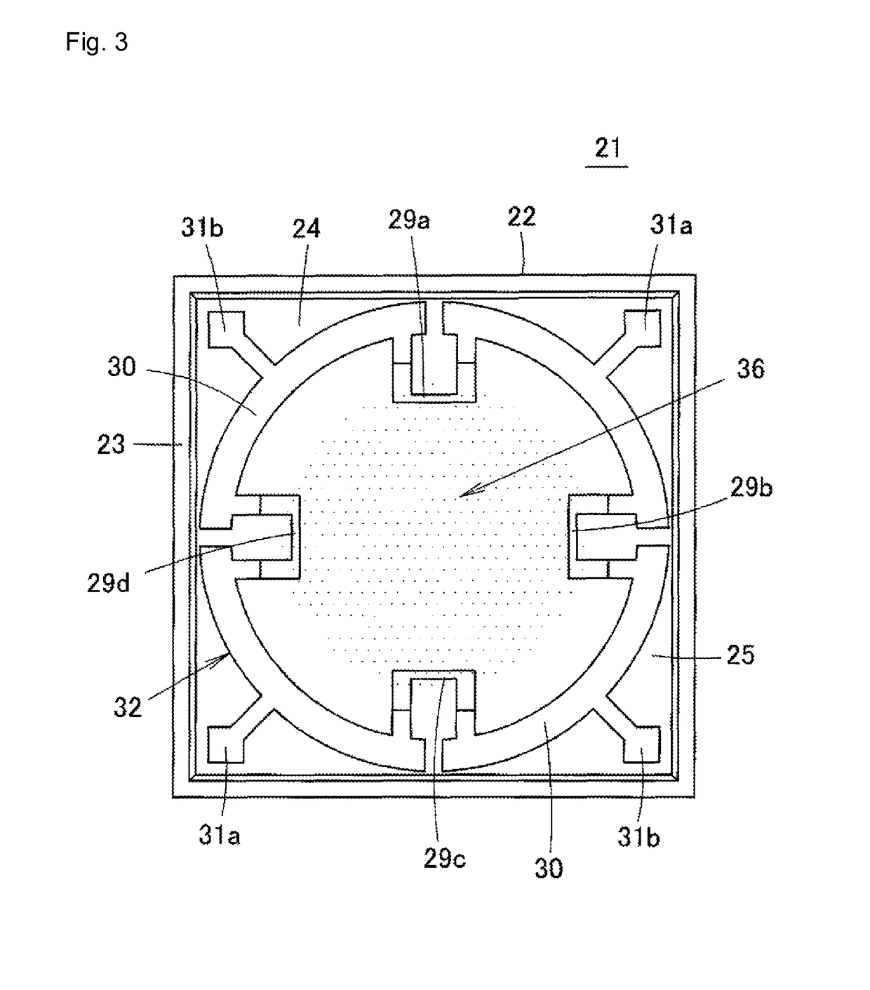
[0029]Hereinafter, a surface potential sensor 21 according to the first embodiment of the present invention will be described with reference to FIGS. 2, 3 and 4. FIG. 2 is a schematic sectional view of a surface potential sensor 21 according to the first embodiment of the present invention, FIG. 3 is a bottom view of a surface potential sensor 21, and FIG. 4 is a circuit diagram showing a distortion quantity detecting unit 32 in the surface potential sensor 21.
[0030]As shown in FIG. 2, a support 23 with a relatively large thickness is provided on an outer peripheral portion of the lower surface of a semiconductor substrate 22 such as a silicon substrate, and a recessed portion 24 surrounded by the support 23 is formed on the lower surface of the semiconductor substrate 22. A thin-film diaphragm 25 (semiconductor layer) located on the recessed portion 24 is floating in a space through support by the support 23. A metal film 26 is formed on the upper surface of the semiconductor subst...
second embodiment
[0064]FIG. 5 is a schematic sectional view showing a surface potential sensor 45 according to a second embodiment of the present invention. In this surface potential sensor 45, a recessed portion 24 is formed by etching on the lower surface of a semiconductor substrate 22 such as a silicon substrate, and a support 23 is formed therearound. Further, a thin-film diaphragm 25 is formed of the semiconductor substrate 22 on the recessed portion 24, and piezoresistors 29a to 29d are provided on the upper surface of the diaphragm 25. Moreover, the upper surface of the semiconductor substrate 22 is covered by an insulating layer 38 such as an oxide film or a nitride film, on which an electret electrode 28 made up of a metal film 26 and an electret film 27 is formed.
[0065]In this surface potential sensor 45, piezoresistors 29a to 29d are produced on the upper surface of semiconductor substrate 22 (wafer), and further, the insulating layer 38, the metal film 26 and the electret film 27 are se...
third embodiment
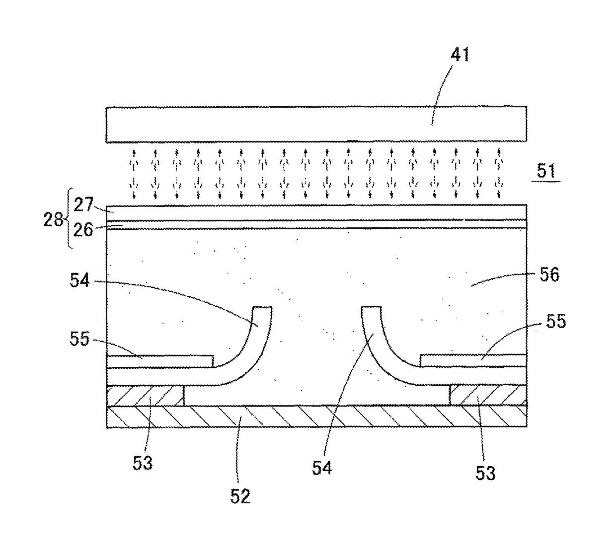
[0066]FIG. 6 is a schematic sectional view of surface potential sensor 51 according to a third embodiment of the present invention. In this surface potential sensor 51, a base 53 is provided on the upper surface of a tabular substrate 52, and a sensing lever 54 (deformable member) is provided on the base 53. The sensing lever 54 has a base portion fixed to the upper surface of the base 53, and a leading end portion curved upward and extended away from the base 53. Further, a strain gauge 55 (distortion quantity detecting device) is fitted to a portion where the largest distortion occurs when force is applied to the sensing lever 54. This sensing lever 54 and the strain gauge 55 constitute an electrostatic force detector. Further, on the upper surface of the substrate 52, an elastic material 56 such as silicon rubber is molded so as to embed the base 53, the sensing lever 54 and the strain gauge 55. The upper surface of the elastic material 56 is formed flat, and the electret electro...
PUM
 Abstract
Description
Claims
Application Information
 - R&D
- Intellectual Property
- Life Sciences
- Materials
- Tech Scout
- Unparalleled Data Quality
- Higher Quality Content
- 60% Fewer Hallucinations
Browse by: Latest US Patents, China's latest patents, Technical Efficacy Thesaurus, Application Domain, Technology Topic, Popular Technical Reports.
© 2025 PatSnap. All rights reserved.Legal|Privacy policy|Modern Slavery Act Transparency Statement|Sitemap|About US| Contact US: help@patsnap.com


