Semiconductor device

A semiconductor and conductive layer technology, applied in the direction of semiconductor devices, semiconductor/solid-state device parts, electric solid-state devices, etc., can solve the problems of increasing the number of manufacturing steps, damaging the components themselves, and increasing costs.

Inactive Publication Date: 2007-04-04
SEMICON ENERGY LAB CO LTD
View PDF2 Cites 1 Cited by
  • Summary
  • Abstract
  • Description
  • Claims
  • Application Information

AI Technical Summary

Problems solved by technology

For this reason, the following problems arise, that is, the size of the antenna is limited in the semiconductor device with built-in antenna, and this will shorten the communication distance, etc.
In addition, there is a problem that the size and / or type of storage containers etc. are limited due to the limitation of the component area
[0009] Furthermore, when the element area is small, it is not possible to ensure a wide area for forming terminals. Therefore, in addition to the above-mentioned limitations, it is also necessary to find ways to provide terminals on the element with insulating layers interposed therebetween.
For this reason, there is a problem that the number of steps for manufacturing components will increase, which in turn becomes one of the main causes of yield reduction or cost increase
[0010] In addition, when the number of terminals is small, when the antenna material and the terminal are pressure-bonded, the load is concentrated on the terminal part and the element itself is damaged, or the load applied to each terminal is uneven, which is a major cause of yield reduction.

Method used


Image

  • Semiconductor device
  • Semiconductor device
  • Semiconductor device

Examples


Embodiment approach 1

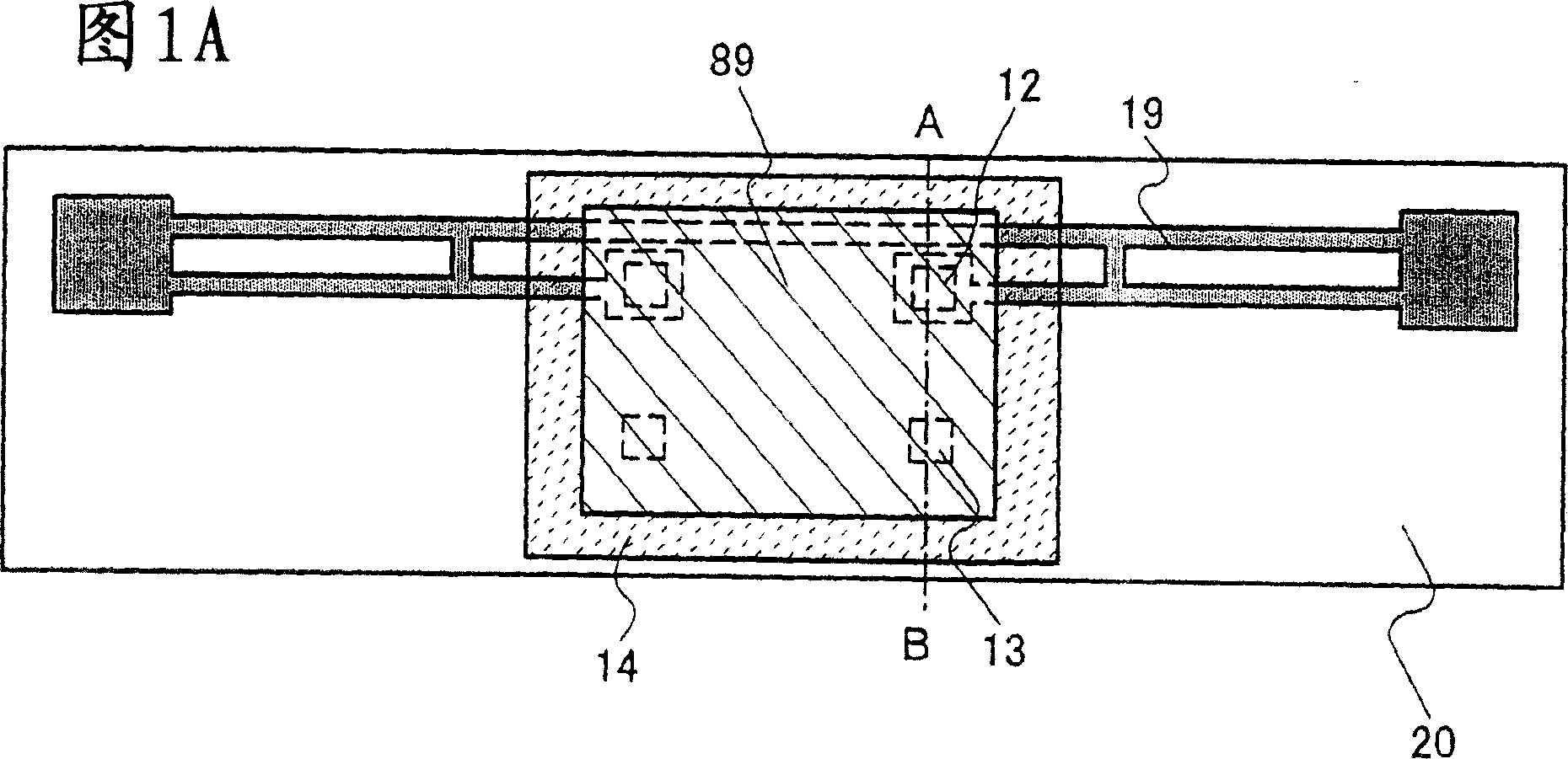
[0052] With reference to FIGS. 1A and 1B and FIGS. 2A and 2B, the structure of the semiconductor device in this embodiment will be described. FIG. 1B is a cross-sectional view from point A to point B in the top view of FIG. 1A. 2B is a cross-sectional view from point A to point B in the plan view of FIG. 2A.

[0053] The substrate 89 and the substrate 20 are arranged such that one surface of the substrate 89 is opposite to one surface of the substrate 20. A layer 11 having integrated circuits is formed on one surface of the substrate 89 (refer to FIGS. 1B and 2B). In addition, on the layer 11 having the integrated circuit, a terminal 12 electrically connected to the wiring included in the layer 11 having the integrated circuit is provided. Note that the layer 11 with integrated circuits includes a plurality of transistors. In addition, the terminal 12 is electrically connected to a conductive layer 19 that functions as an antenna formed on one surface of the substrate 20 via a con...

Embodiment approach 2

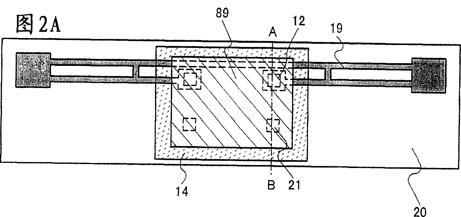
[0059] In this embodiment mode, the structure of a semiconductor device having a different shape from the semiconductor device shown in Embodiment Mode 1 will be described using FIGS. 3A and 3B. The difference between this embodiment mode and the structure shown in Embodiment Mode 1 is that in addition to the conductive layer functioning as an antenna, a conductive layer made of conductive material is provided on the substrate on one surface of the conductive layer functioning as an antenna. Layers of composition. Note that the description of the same parts as in Embodiment 1 will be omitted.

[0060] As shown in FIG. 3A and FIG. 3B, the element of the present invention has a dummy terminal 13 on a layer 11 having an integrated circuit. Note that with regard to the number of dummy terminals and the positions where they are formed, the present invention is not limited to the structure described in the drawings. In other words, one more dummy terminals 13 may be provided, and the pl...

Embodiment approach 3

[0066]The embodiment of the present invention will be described with reference to FIGS. 4A and 4B. In this embodiment mode, a structure of a semiconductor device having a shape different from that in Embodiment Mode 1 and Embodiment Mode 2 will be described. This embodiment is different from Embodiment 1 and Embodiment 2 in the shape of the conductive layer functioning as an antenna, and in addition to the terminals electrically connected to the conductive layer functioning as an antenna, it also has a plurality of conductive layers that are electrically connected to the conductive layer functioning as an antenna. Connected terminal (hereinafter referred to as auxiliary terminal). Note that the description of the same parts as in Embodiment 1 will be omitted.

[0067] As shown in FIGS. 4A and 4B, the layer 11 having the integrated circuit has an auxiliary terminal 24. The auxiliary terminal 24 is electrically connected to the wiring included in the layer 11 having the integrated c...


PUM


Abstract

The present invention provides a semiconductor device of which mass production is possible and the structure is different from that of a conventional small-size element. In addition, it is an object of the invention to provide a structure of a semiconductor device of which the strength can be improved, destruction of an element in manufacturing can be suppressed, and the reliability and yield are high, and a manufacturing method of the semiconductor device. The invention includes a layer having an integrated circuit, a first terminal which is formed over the layer having the integrated circuit and is electrically connected to the layer having the integrated circuit, a conductive layer which functions as an antenna, which is formed over the first terminal and is electrically connected to the first terminal, and a second terminal which is formed over the layer having the integrated circuit and is not electrically connected to the layer having the integrated circuit, the conductive layer which functions as the antenna, and the first terminal.

Description

Technical field [0001] The present invention relates to a semiconductor device mounted with a thin film integrated circuit, wherein the thin film integrated circuit has a memory, a microprocessor (central processing unit, MPU), etc. and is as thin as paper and has bending flexibility. The present invention also relates to a non-contact type semiconductor device with the thin film integrated circuit and antenna, which is mainly used to identify cards, labels, tags, etc., for people, animals, plants, commodities, banknotes, and the like. Background technique [0002] In recent years, research on semiconductor devices capable of transmitting / receiving data has been a hot spot. Such semiconductor devices are called IC chips, RF tags, wireless tags, electronic tags, wireless processors, wireless memories, and the like. Although most of the semiconductor devices that have been put into practical use are formed of single crystal silicon substrates. However, the commercialization of thin...

Claims


Application Information

Patent Timeline
Patent Type & Authority Applications(China)
IPC IPC(8): G06K19/077H01L27/02H01L23/522H01L23/48
CPCH01L23/5389H01L23/49855H01L2924/01046H01L2224/16H01L2924/01078H01L2924/01079H01L2924/01004G06K19/0775H01L2924/04941H01L2924/01077H01L2223/6677G06K19/07749H01L2924/12044H01L2924/00
Inventor 楠本直人高桥秀和小林由佳
Owner SEMICON ENERGY LAB CO LTD
Why Eureka
Try Eureka