Contact image sensor and method for manufacturing the same

An image sensor, contact technology, applied in the direction of image communication, electrical components, etc., can solve problems such as uniformity, and achieve the effect of easy online adjustment and large amount of light

Inactive Publication Date: 2007-03-14
NIPPON SHEET GLASS CO LTD
View PDF3 Cites 2 Cited by
  • Summary
  • Abstract
  • Description
  • Claims
  • Application Information

AI Technical Summary

Problems solved by technology

This is because when forming a lens array plate by injection molding, it is difficult to make the dimensions (especially plate thickness) and lens characteristics (optical axis direction, lens pitch, curvature, etc.) uniform throughout the molded body

Method used


Image

  • Contact image sensor and method for manufacturing the same
  • Contact image sensor and method for manufacturing the same
  • Contact image sensor and method for manufacturing the same

Examples


Embodiment 1

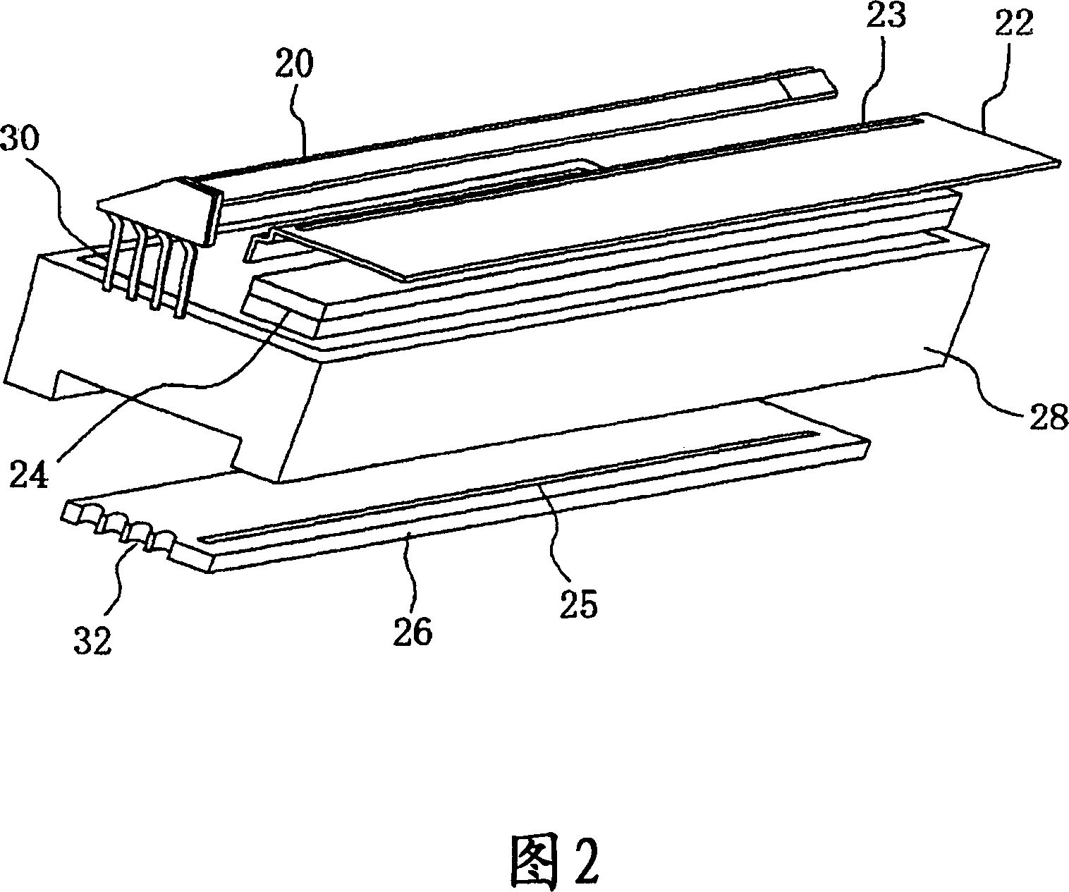
[0049] Fig. 2 is an exploded perspective view of a contact image sensor. This contact image sensor is made up of the following parts: light source 20, slit 22, the upright equal-magnification lens 24 that is made of overlapping two plate microlens arrays 24A and 24B, the light-receiving element array 25 that has installed light-receiving element array 24. The element array substrate 26, and the case 28 for accommodating the above-mentioned components.

[0050] The light source 20 is a linear lighting device, and as such a linear lighting device, there are those in which the array of light emitting elements extends in the main scanning direction, those in which light emitting elements are provided at the ends of the linear light guide, and the like.

[0051] In addition, in this embodiment, an example in which light-emitting elements composed of three light-emitting diodes (LEDs) of R color, G color, and B color are provided at the end of the linear light guide will be describe...

Embodiment 2

[0073] The contact image sensor of the second embodiment can be realized by the configuration shown in FIG. 2, and the description of the same constituent elements will be omitted. In Embodiment 2, a method of adjusting the position of the light-receiving element array substrate which is different from Embodiment 1 will be described. The method is as follows: firstly, the light-receiving element array receives the reflected light of a reference original (such as a white original) with uniform brightness distribution corresponding to the light distribution in the main scanning direction of the light source, and then detects the sensor corresponding to the light distribution in the main scanning direction of the light source. output. Next, in order to reduce the detected difference in sensor output in the main scanning direction, the position of the light receiving element array substrate is adjusted by inclining the position of the light receiving element array in the sub scann...


PUM


Abstract

In order to prevent double ghost, a contact image sensor having a structure which is convenient to adjust the position of the light-receiving element array substrate is provided. The contact image sensor is composed of a light source 20 having a light-receiving element array, a slit 22, a lens 24, a light-receiving element array substrate 26 provided with a light-receiving element array 25, and a housing 28 holding the above parts. Four leads 30 for power supply are provided at one end of the light source 20. Four U-shape grooves 32 for allowing leads 30 to pass through are formed at one end of the light-receiving element array substrate 26. The size of the grooves 32 is left with sufficient space with respect to the thickness of the lead 30.

Description

technical field [0001] The present invention relates to a method for adjusting the position of a light-receiving element array substrate included in a contact image sensor in a sub-scanning direction, a method for manufacturing a contact image sensor, and a contact image sensor. Background technique [0002] A contact image sensor capable of reading document information is composed of a light source, a lens, a light receiving element (CCD, etc.), and a housing (casing) for storing them. The contact image sensor adopts the following structure: the original is irradiated with the light emitted from the light source, the reflected light of the original is collected by the lens, and then received by the light receiving element. When the reflected light from the original surface enters the lens and is absorbed by the light-receiving element, ghost images often occur due to the composition of the optical system, which is the cause of poor image quality. Ghosting is a phenomenon i...

Claims


Application Information

Patent Timeline
Patent Type & Authority Applications(China)
IPC IPC(8): H04N1/028
Inventor 齐藤富久吉田治信脇坂政英北岡正树
Owner NIPPON SHEET GLASS CO LTD
Why Eureka
Try Eureka