
Method and apparatus for reduced noise band switching circuits

By using a capacitive voltage dividing circuit and a bias control circuit in the VCO, the problem of noise in the band conversion circuit is solved, low phase noise signal output is achieved, and the signal quality in wireless communication is improved.

Inactive Publication Date: 2007-01-17
SIRIFIC WIRELESS CORP
View PDF1 Cites 7 Cited by
  • Summary
  • Abstract
  • Description
  • Claims
  • Application Information

AI Technical Summary

Problems solved by technology

In a typical band switching circuit, the bias voltage of the amplifier or the bias voltage of the oscillator circuit introduces noise, which results in phase noise in the output of the VCO

Method used


Image

  • Method and apparatus for reduced noise band switching circuits
  • Method and apparatus for reduced noise band switching circuits
  • Method and apparatus for reduced noise band switching circuits

Examples


Embodiment Construction

[0021] In general, the present invention provides a method and apparatus for implementing a noise-reduced band switching circuit.

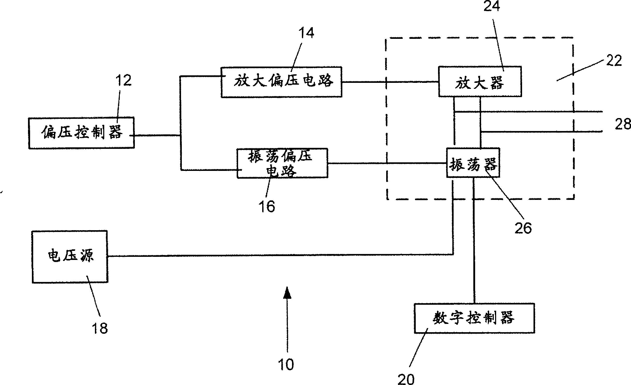
[0022] Referring to FIG. 1 , it shows a schematic diagram of a VCO in the prior art. The VCO 10 includes a bias controller 12 connected to an amplification bias circuit 14 and an oscillation bias circuit 16 . Voltage source 18 and digital controller 20 are connected to VCO core 22 along with amplification bias circuit 14 and oscillation bias circuit 16 . VCO core 22 includes amplifier 24 and oscillator 26 . The output from the amplifier 24 and the output from the oscillator 26 are delivered as an output voltage 28 .

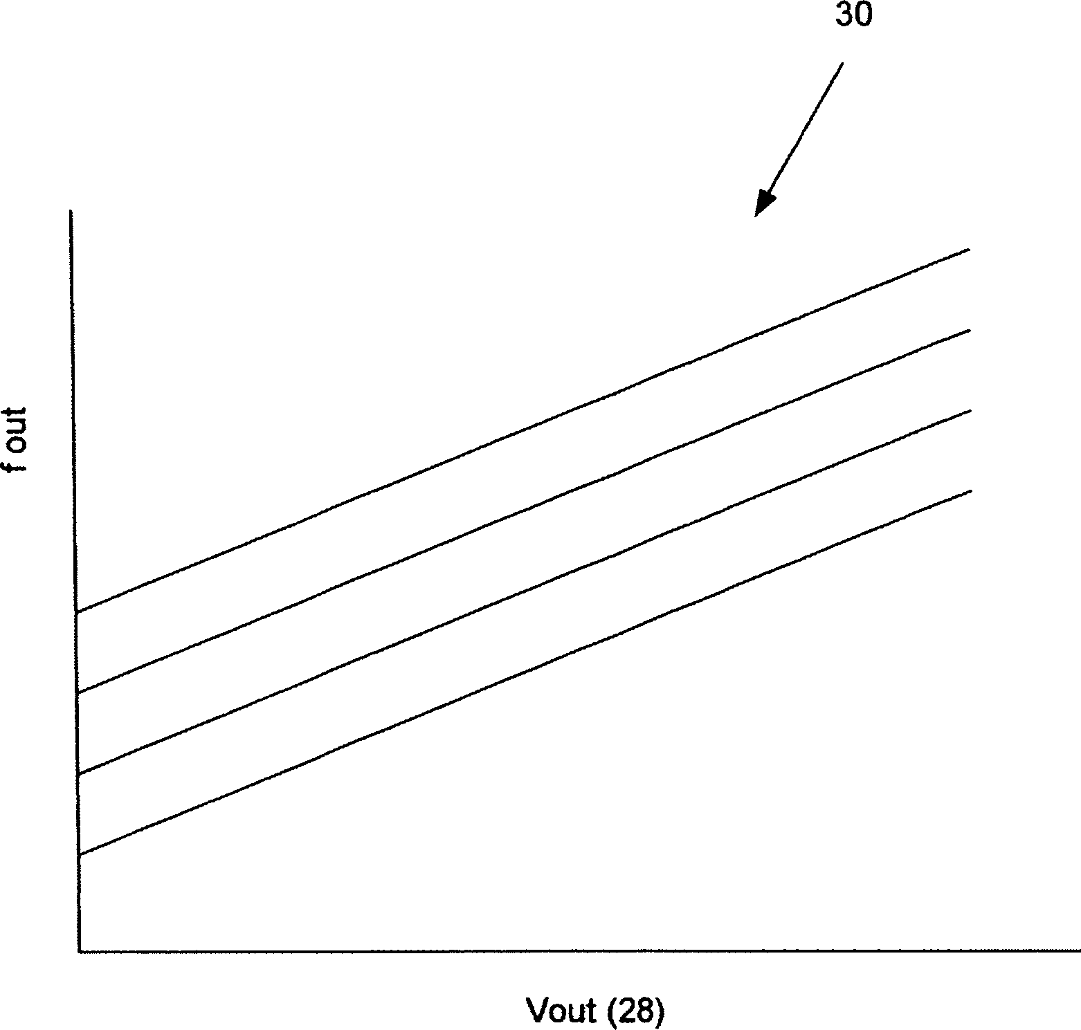
[0023] FIG. 2 provides a graph 30 of output voltage 28 versus frequency while VCO 10 is operating.

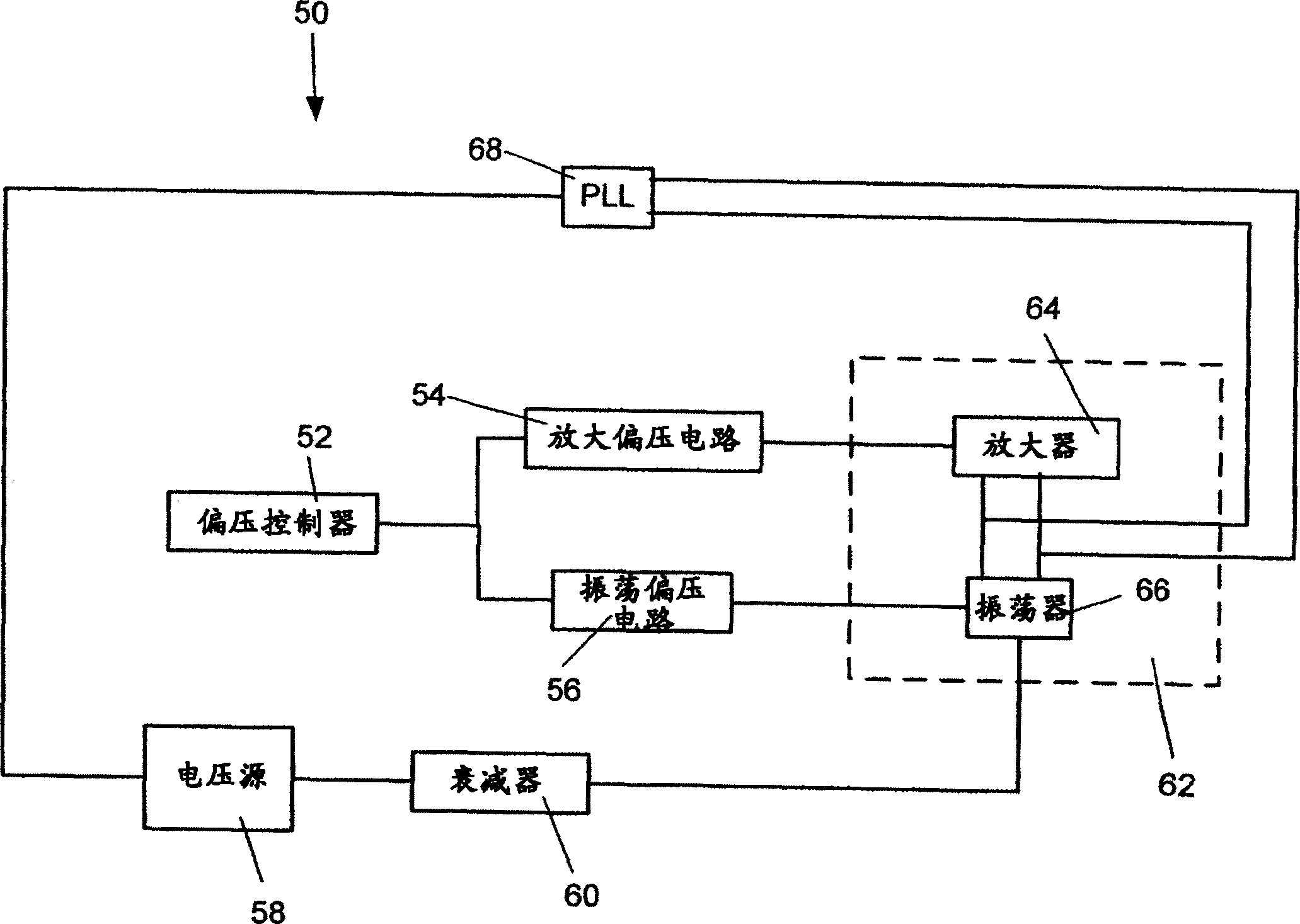
[0024] see image 3 , shows a device for implementing a low-noise band switching circuit. The device targets VCOs that generate signals in wireless radio frequency (RF) applications. The device or VCO 50 includes a bias controlle...


PUM


Abstract

A low-phase noise voltage control oscillator (VCO) comprising a voltage source for supplying control voltage to the VCO core; a phase lock loop, having an output connected to an input of the voltage source; a VCO core, including an amplifier circuit with noiseless biasing and a tank circuit with noiseless biasing of the varactors; having an output connected to an input of the phase lock loop; and an attenuator, located between the voltage source and the VCO core, for reducing phase noise from the voltage source to the VCO core.

Description

technical field [0001] The present invention relates generally to the field of oscillators. More particularly, the present invention relates to voltage controlled oscillators (VCOs) for generating signals in wireless communication applications. Background technique [0002] A VCO is a circuit that uses amplification, feedback, and resonance circuits to create an oscillating signal to generate a repetitive voltage waveform so that its output frequency is proportional to its input voltage. [0003] In wireless communication applications, VCOs operate over a wide frequency range. A VCO generally includes a tank circuit and an amplifier circuit, the operations of which are well known. Viasing for these circuits is also well known and described in US Patent No 6,674,333 to Peckham et al., which describes a method of operating a band-variable VCO in different frequency bands . In a typical band switching circuit, the bias voltage of the amplifier or the bias voltage of the osc...

Claims


Application Information

Patent Timeline
Patent Type & Authority Applications(China)
IPC IPC(8): H03B5/02H03B5/04H03B5/12H03L7/099
CPCH03B5/1228H03B2200/0088H03B5/1293H03B5/124H03L7/099H03B5/1212H03B5/04H03L7/08
Inventor 弗洛达迈·雅弗斯基塔基德·曼库詹姆斯·韦
Owner SIRIFIC WIRELESS CORP
Learn More