Display device and control method thereod
A display device and switching element technology, applied in static indicators, instruments, etc., can solve problems such as inability to level shift, lagging in the establishment of output voltage, and increased on-resistance of NMOS3, and achieve stable driving and low power consumption. Effect
- Summary
- Abstract
- Description
- Claims
- Application Information
AI Technical Summary
Problems solved by technology
Method used
Image

Examples
Embodiment 1
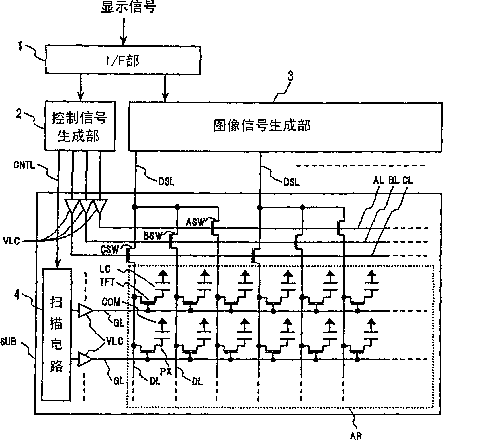
[0045] figure 1 It is a schematic configuration diagram showing the whole of the liquid crystal display device of the present invention, and includes one transparent insulating substrate SUB among a pair of transparent insulating substrates (for example, glass substrates) arranged to face each other with liquid crystal interposed therebetween. The center portion of the surface of the transparent insulating substrate SUB on the liquid crystal side except for the periphery is the display area AR.
[0046] In this display area AR, there is formed a figure 1 Among them, a plurality of gate signal lines GL extending in the x direction and juxtaposed in the y direction, and a plurality of drain signal lines DL extending in the y direction and juxtaposed in the x direction.
[0047] Here, each area surrounded by two adjacent gate signal lines GL and two adjacent drain signal lines DL constitutes a pixel area, in which a thin film transistor TFT and a pixel electrode PX are provide...
Embodiment 2
[0152] Below, for implementing figure 1 Embodiment 2 of the present invention of the voltage level converter VLC of the liquid crystal display device shown will be described.
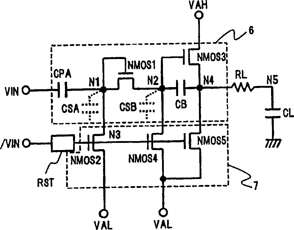
[0153] Figure 7 The circuit structure of the voltage level converter VLC of this embodiment is shown. The voltage level shifter VLC is described in Example 1 by combining the 2 figure 2 The voltage level translators shown are connected to form a circuit.
[0154] Figure 7 The voltage level shifter shown is the first stage converter with figure 2 The configuration of the voltage level shifting circuit of the first embodiment shown is the same, and therefore description thereof will be omitted.
[0155] In the second-stage voltage level shifter, no capacitor equivalent to the capacitor CPA in the first-stage level shifter is provided, and the node N4, which is the output signal of the first-stage voltage level shifter, becomes the second-stage voltage level shifter. The input signal of the leve...
Embodiment 3
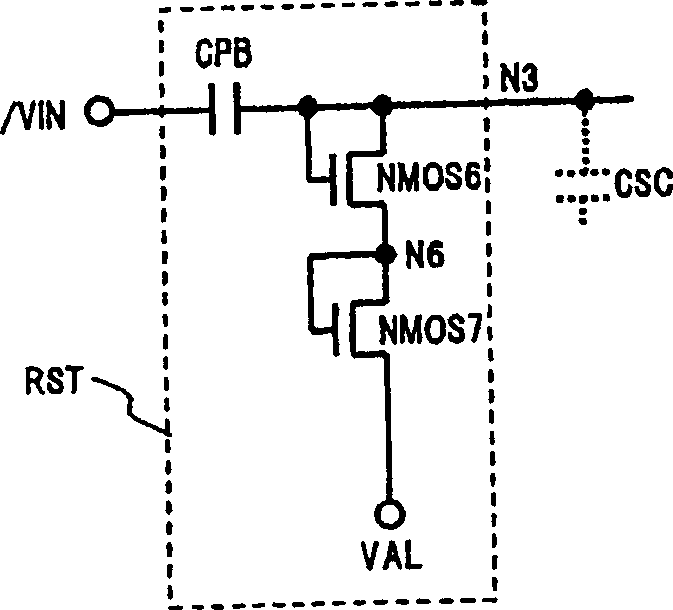
[0188] Below, for implementing figure 1 Embodiment 3 of the present invention of the voltage level converter VLC of the liquid crystal display device shown will be described. Figure 9 The circuit structure of the voltage level converter VLC of this embodiment is shown.
[0189] Figure 9 The voltage level shifter VLC shown includes: a voltage level shifting block consisting of two stages (circuit structure and Figure 7 roughly the same), which is used to improve the rising speed of the output potential of the voltage level conversion circuit; figure 2 roughly the same), which is used to improve the output potential drop speed and generate a high-amplitude gate voltage required to reduce the on-resistance of the MOS transistor connected to the low-potential power supply VAL in the output stage circuit of the voltage level conversion block.
[0190] Next, the connection structure of each element will be described. exist Figure 9 In the voltage level shifter shown, the ...
PUM
 Abstract
Description
Claims
Application Information
 - Generate Ideas
- Intellectual Property
- Life Sciences
- Materials
- Tech Scout
- Unparalleled Data Quality
- Higher Quality Content
- 60% Fewer Hallucinations
Browse by: Latest US Patents, China's latest patents, Technical Efficacy Thesaurus, Application Domain, Technology Topic, Popular Technical Reports.
© 2025 PatSnap. All rights reserved.Legal|Privacy policy|Modern Slavery Act Transparency Statement|Sitemap|About US| Contact US: help@patsnap.com