
Gain control circuit capable of reducing change in gain due to variation of ambient temperature

A gain control circuit and gain change technology, which are applied in gain control, improvement of control circuit by reducing distortion, amplification control, etc., can solve the problems of transistor 1 gain change and other problems, and achieve the effect of suppressing current change

Inactive Publication Date: 2006-11-15
ALPS ALPINE CO LTD
View PDF0 Cites 3 Cited by
  • Summary
  • Abstract
  • Description
  • Claims
  • Application Information

AI Technical Summary

Problems solved by technology

[0006] Even if the control voltage is constant, if the ambient temperature changes, the DC bias current flowing through the variable resistance element 5 changes accordingly, and the gain of the transistor 1 changes.

Method used


Image

  • Gain control circuit capable of reducing change in gain due to variation of ambient temperature
  • Gain control circuit capable of reducing change in gain due to variation of ambient temperature
  • Gain control circuit capable of reducing change in gain due to variation of ambient temperature

Examples


Embodiment Construction

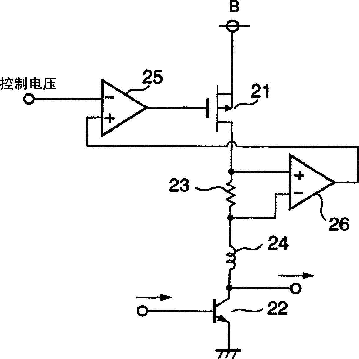
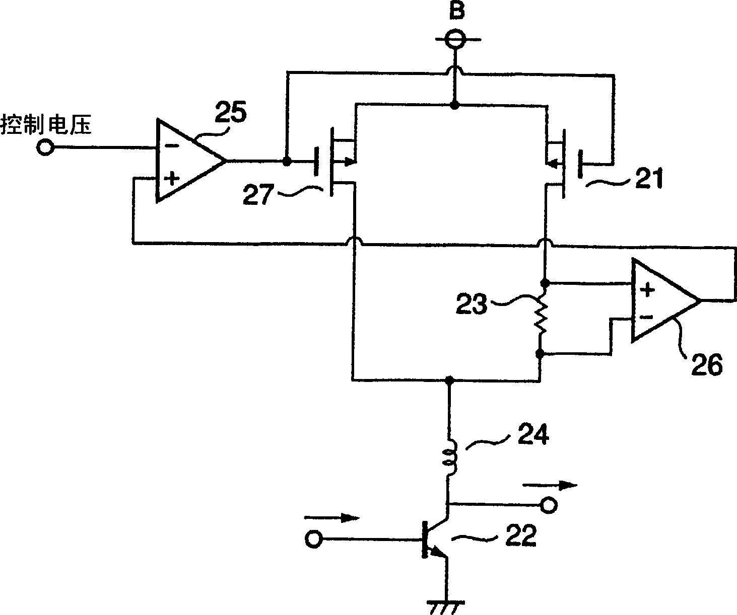
[0022] figure 1 The first embodiment of the present invention is shown. A power supply voltage is supplied to the amplifying transistor 22 via the first variable resistance unit 21 connected to the power supply terminal B. Between the first variable resistance unit 21 and the amplifying transistor 22 , a current detecting resistor 23 having a small resistance value is inserted, and a load 24 is inserted between the current detecting resistor 23 and the collector of the amplifying transistor 22 . The first variable resistance unit 21 is composed of a 3-terminal semiconductor element having a current input terminal, a current output terminal and a control terminal, and controls the current flowing through the voltage difference between the current input terminal and the control terminal, for example, by C - a first P-channel type field effect transistor made of MOS. Furthermore, the source as the current input terminal is connected to the power supply terminal B, and the drai...


PUM


Abstract

A gain control circuit capable of keeping a constant gain without being affected by ambient temperature includes a variable resistor element connected to a power supply terminal, a control unit for controlling the resistance value of the variable resistor element on the basis of a gain control voltage, an amplifying transistor that is supplied with a power supply voltage through the variable resistor element, a current detecting resistor that is interposed between the variable resistor element and a collector of the amplifying transistor, and a voltage detecting unit that detects a drop dropped by the current detecting resistor. The dropped voltage detected by the voltage detecting unit is fed back to the control unit to control the resistance value of the variable resistor element such that a current flowing through the current detecting resistor does not vary.

Description

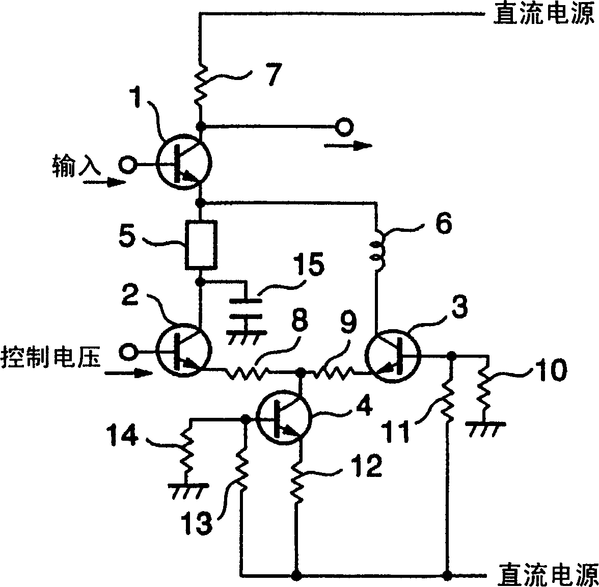
technical field [0001] In particular, the present invention relates to gain control circuits suitable for mobile phone power amplifiers and the like. Background technique [0002] image 3 The conventional gain control circuit shown is a combination of a differential circuit of an emitter-grounded amplifier circuit. The amplifying circuit with the emitter grounded is composed of a transistor 1, a variable resistance element 5 of a PIN diode, and a resistor 7. The DC bias portion of the emitter current of transistor 1 is split differentially in transistors 2,3. The emitter current is stabilized by transistor 4 . The input signal is amplified by transistor 1. Since the signal portion is blocked by the inductor 6 on the emitter side of the transistor 1 , the gain is determined by the ratio of the AC resistance of the collector resistor 7 and the variable resistance element 5 . [0003] The AC resistance of the variable resistance element 5 changes in inverse proportion to t...

Claims


Application Information

Patent Timeline
Patent Type & Authority Applications(China)
IPC IPC(8): H03G3/20H03G3/30
CPCH03F1/30H03F1/302H03F3/04H03F3/24H03F3/45475H03F2200/447H03F2200/451H03F2200/504H03G1/04
Inventor 浅野正一青木一晴
Owner ALPS ALPINE CO LTD
Learn More