Plasma display device, plasma display panel and producing method

A display panel and display device technology, which is applied in the direction of AC plasma display panels, cold cathode manufacturing, electrode system manufacturing, etc., can solve the problems of no longer smooth interaction, poor image jumping characteristics, unstable discharge, etc., to prevent power Effects of loss, brightness enhancement, contrast characteristic improvement

Inactive Publication Date: 2006-08-09
LG ELECTRONICS INC
View PDF0 Cites 0 Cited by
  • Summary
  • Abstract
  • Description
  • Claims
  • Application Information

AI Technical Summary

Problems solved by technology

However, although this partition wall structure may improve the exhaust characteristics of the plasma display panel, there is a difference in the permittivity between the first partition wall 21a and the second partition wall 21b separating the discharge cells, and there is a problem of unstable discharge.
And when the bus electrodes constituting the scan electrodes and the sustain electrodes are located on the partition walls in the row direction of the panel, the interaction with the address electrodes formed on the lower substrate becomes no longer smooth, and the image jitter characteristics deteriorate.
That is, ineffective power that is not used for driving the actual circuit is generated between the address electrode and the bus electrode, resulting in power loss

Method used


Image

  • Plasma display device, plasma display panel and producing method
  • Plasma display device, plasma display panel and producing method
  • Plasma display device, plasma display panel and producing method

Examples


no. 1 approach

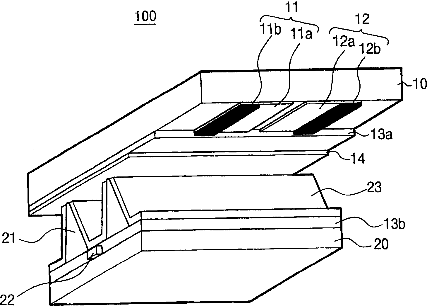
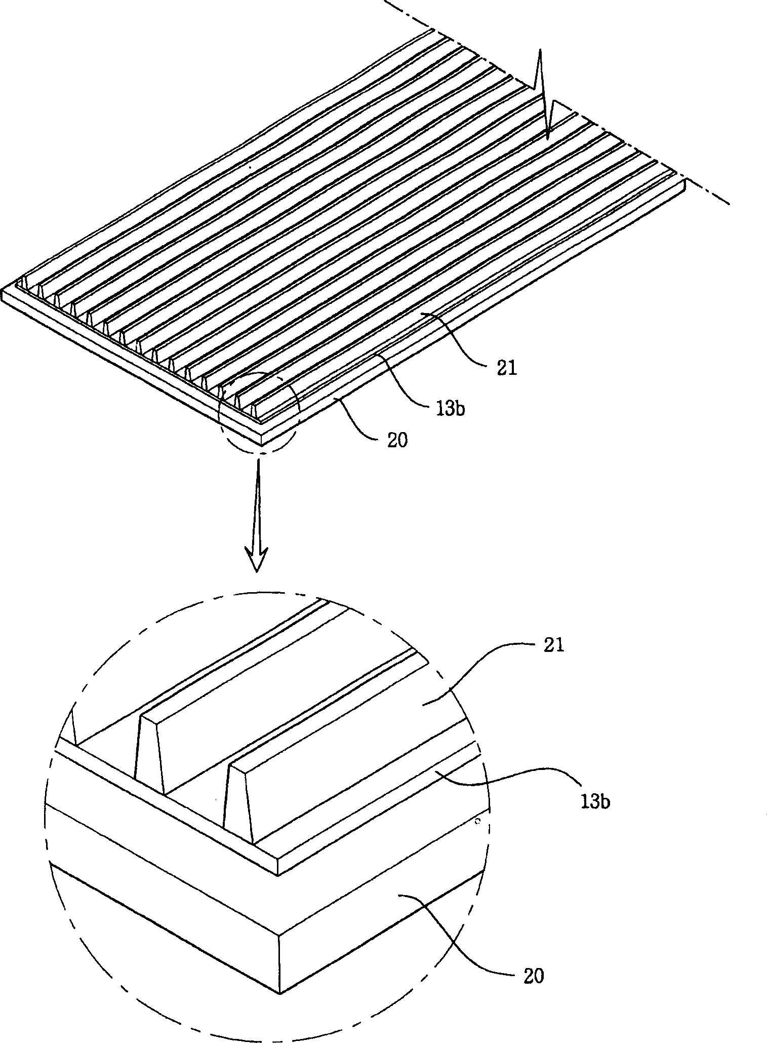
[0033] FIG. 5 is a perspective view showing a partition wall structure of the plasma display panel according to the first embodiment of the present invention. The following description will be made before looking at FIG. 5. Although not shown in the figure, the plasma display panel according to the first embodiment of the present invention is the same as the prior art. The substrates are bonded and formed at intervals.

[0034] The front substrate has sustain electrodes formed by pairing scan electrodes and sustain electrodes on the top of the front glass, and an upper dielectric layer is laminated on the front glass where the scan electrodes and sustain electrodes are arranged in parallel to limit the discharge current. In addition, a protective layer of evaporated magnesium oxide (MgO) is formed on the upper dielectric layer, and the protective layer is used to prevent damage to the upper dielectric layer due to sputtering (sputtering) generated during plasma discharge, and ...

no. 2 approach

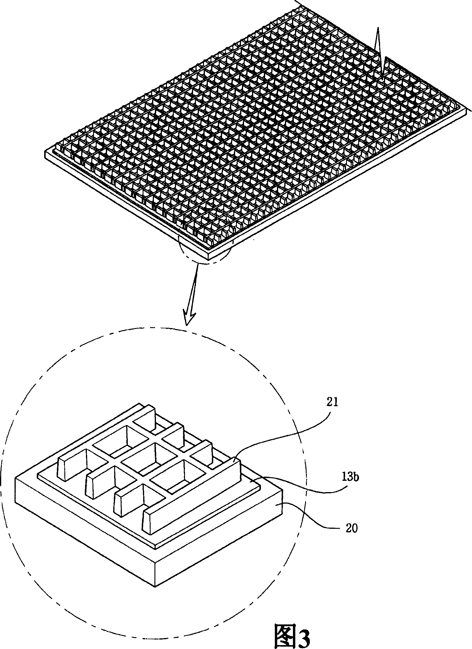
[0043] Figure 6 It is a perspective view showing the partition wall structure of the plasma display panel in the second embodiment of the present invention. Although not shown in the drawings, the plasma display panel according to the second embodiment of the present invention has a structure corresponding to the structure of the plasma display panel according to the first embodiment of the present invention described above. However, the partition walls formed in the plasma display panel according to the second embodiment of the present invention are as follows: Figure 6 As shown, the lower dielectric layer 130b' on the back glass 200' is configured to be surrounded by row ribs (row rib, 210a') and column ribs (column rib, 210b') to separate the Well Type of discharge cells. ), wherein the row partition wall 210a' and the column partition wall 210b' have different heights from each other. In this case, the row partition walls 210a' and the column partition walls 210b' are ...


PUM


Abstract

There are provided a plasma display apparatus and a manufacturing method thereof. A PDP according to a first embodiment of the present invention includes: row ribs (210a) and column ribs (210b) with a height different from that of the row ribs (210a), wherein a permittivity of higher ones of the row ribs (210a) and the column ribs (210b) is lower than that of lower ones of the row ribs (210a) and the column ribs (210b). A PDP according to a second embodiment of the present invention includes: row ribs (210a) and column ribs (210b) with a height different from that of the row ribs (210a), wherein a permittivity of higher ones of the row ribs (210a) and the column ribs (210b) is lower than that of lower ones of the row ribs (210a) and the column ribs (210b) and the higher ribs are made of at least two materials with different permittivities. Also, the method for manufacturing the PDP, the PDP including discharge cells partitioned by row ribs (210a) and column ribs (210b), wherein a method for forming the row ribs (210a) and the column ribs (210b) including: (a) forming a paste for the row ribs (210a) and the column ribs (210b) on a dielectric layer formed on a glass; (b) forming a pattern for forming the row ribs (210a) and the column ribs (210b) on the paste for the row ribs (210a) and the column ribs (210b); and (c) forming a material having a permittivity lower than that of the paste for forming the column ribs (210b), with a predetermined height on the column ribs (210b).

Description

technical field [0001] The present invention relates to a plasma display panel, in particular to a plasma display device, a plasma display panel and a manufacturing method thereof, which can improve partition walls separating discharge cells of the plasma display panel to improve discharge efficiency. Background technique [0002] Generally, in a plasma display panel, a partition wall formed between a front panel and a back panel constitutes a discharge cell, and each cell includes neon (Ne), helium (He) or a mixed gas of neon and helium (Ne+ He) the main discharge gas and a small amount of xenon inert gas for charging. When the high-frequency voltage is turned into a discharge, the inert gas generates vacuum ultraviolet rays (Vacuum Ultraviolet Rays), which makes the phosphors formed between the partition walls emit light, thereby displaying images. Such a plasma display panel has a thin and light structure, and thus is attracting attention as a next-generation display dev...

Claims


Application Information

Patent Timeline
Patent Type & Authority Applications(China)
IPC IPC(8): H01J17/16H01J17/04H01J17/49H01J9/02H01J9/24H01J11/22H01J11/24H01J11/34H01J11/36
CPCH01J2211/361H01J11/36H01J2211/444H01J11/12H01J9/242H01J11/38H01J11/44
Inventor 郑真熙
Owner LG ELECTRONICS INC
Why Eureka
Try Eureka