LED structure

A light-emitting diode, N-type technology, applied in electrical components, circuits, semiconductor devices, etc., can solve the problems of maintaining light-emitting/illumination performance, insufficient light-emitting diode structure, etc.

Active Publication Date: 2006-06-14
FORMOSA EPITAXY INCORPORATION +1
View PDF0 Cites 7 Cited by
  • Summary
  • Abstract
  • Description
  • Claims
  • Application Information

AI Technical Summary

Problems solved by technology

[0011] However, as in Figure 4 The characteristic curve (a) and Figure 5 As shown in the characteristic curve (a): the reverse voltage and antistatic characteristics of the conventional gallium nitride (GaN) light-emitting diode structure are low, which is still not enough to maintain the light-emitting diode structure for a long period of time under strict outdoor environmental conditions. High-level lighting / illumination performance

Method used


Image

  • LED structure
  • LED structure
  • LED structure

Examples


Embodiment Construction

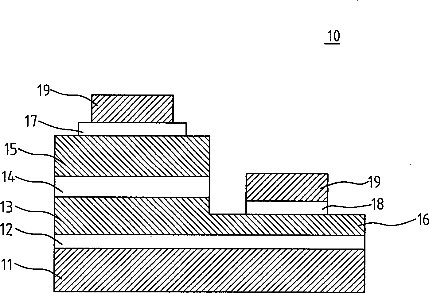
[0054] Embodiments of the present invention will now be described with reference to the drawings. Among them, different parts of some components are not drawn according to actual size. Certain dimensions are shown exaggerated in relation to other parts to provide a clearer description and to assist those skilled in the art in understanding the present invention.

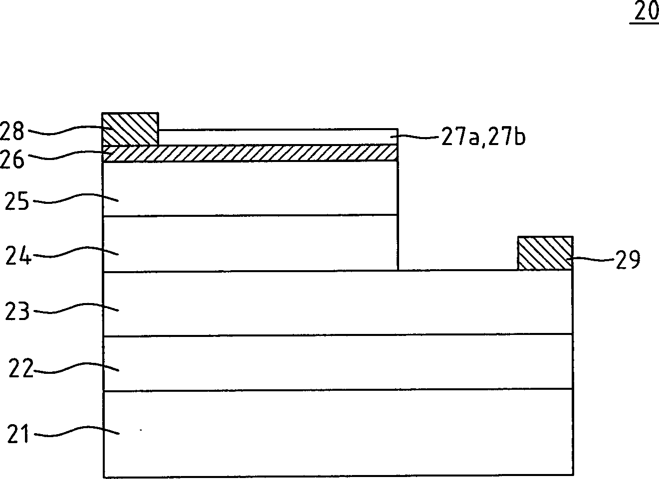
[0055] First, please refer to figure 2 . figure 2 shows a gallium nitride-based light-emitting diode structure 20 according to an embodiment of the present invention with improved reverse voltage and antistatic functions, which includes: a substrate 21, a buffer layer 22, an N-type gallium nitride-based (GaN) layer 23, a light-emitting Stack layer 24 , P-type gallium nitride (GaN) layer 25 , digital pass-through layer 26 , transparent conductive layer 27 a or transparent conductive oxide layer 27 b , first ohmic electrode 28 , and second ohmic electrode 29 .

[0056]In the above structure, the bottom layer of th...


PUM

PropertyMeasurementUnit
Thicknessaaaaaaaaaa

Abstract

The invention mainly provides a structure of a GaN light-emitting diode with digital penetrating layer, for overcoming the disadvantages and limits of a light-emitting diode in the existing technique and largely improving reverse voltage-proof and antistatic properties of the GaN light-emitting diode. The invention also provides a device for reducing the resistance between the transparent conductive layer and P-type GaN contact layer arranged in the GaN light-emitting diode, according to a digital penetrating layer between the two layers which can make internal carrier penetration, making an ohm contact state formed between the transparent conductive layer or oxide layer and the P-type GaN contact layer so as to be able to reduce the resistance between them. In addition, the invention provides a material able to make internal carrier penetration. The invention replaces the traditional Ni / Au with a material with excellent visible light photopermeability, such as indium tin oxide as the transparent conductive layer.

Description

technical field [0001] The present invention relates to a gallium nitride-based light-emitting diode, in particular to a gallium-nitride-based light-emitting diode with characteristics of high reverse resistance voltage and high antistatic capability. Background technique [0002] It is understood that there are many types of image displays currently used in the industry, including: displays made of traditional cathode ray tubes (CRTs), liquid crystal displays (LCDs) developed by high-tech technologies in recent years, and displays made of Displays made of light-emitting diodes (LEDs). Generally, liquid crystal displays are suitable for displaying dynamic images, while displays made of light-emitting diodes are suitable for displaying static images. [0003] In the field of light-emitting diodes, the structure of gallium nitride (GaN)-based light-emitting diodes is one of the types of light-emitting diodes that the optoelectronic industry has devoted to research and develop...

Claims


Application Information

Patent Timeline
IPC IPC(8): H01L33/32H01L33/36
Inventor 武良文凃如钦游正璋温子稷简奉任
Owner FORMOSA EPITAXY INCORPORATION
Why Eureka
Try Eureka