
Semiconductor manufacturing apparatus and chemical exchanging method

A technology for chemical reagents and manufacturing devices, applied in semiconductor/solid-state device manufacturing, chemical instruments and methods, cleaning methods using liquids, etc., can solve problems such as mixing new chemical reagents and waste chemical reagents

Inactive Publication Date: 2006-03-01
SEIKO EPSON CORP
View PDF1 Cites 6 Cited by
  • Summary
  • Abstract
  • Description
  • Claims
  • Application Information

AI Technical Summary

Problems solved by technology

However, in this method, new and spent chemicals may be mixed inside the treatment tank

Method used


Image

  • Semiconductor manufacturing apparatus and chemical exchanging method
  • Semiconductor manufacturing apparatus and chemical exchanging method
  • Semiconductor manufacturing apparatus and chemical exchanging method

Examples


no. 1 example

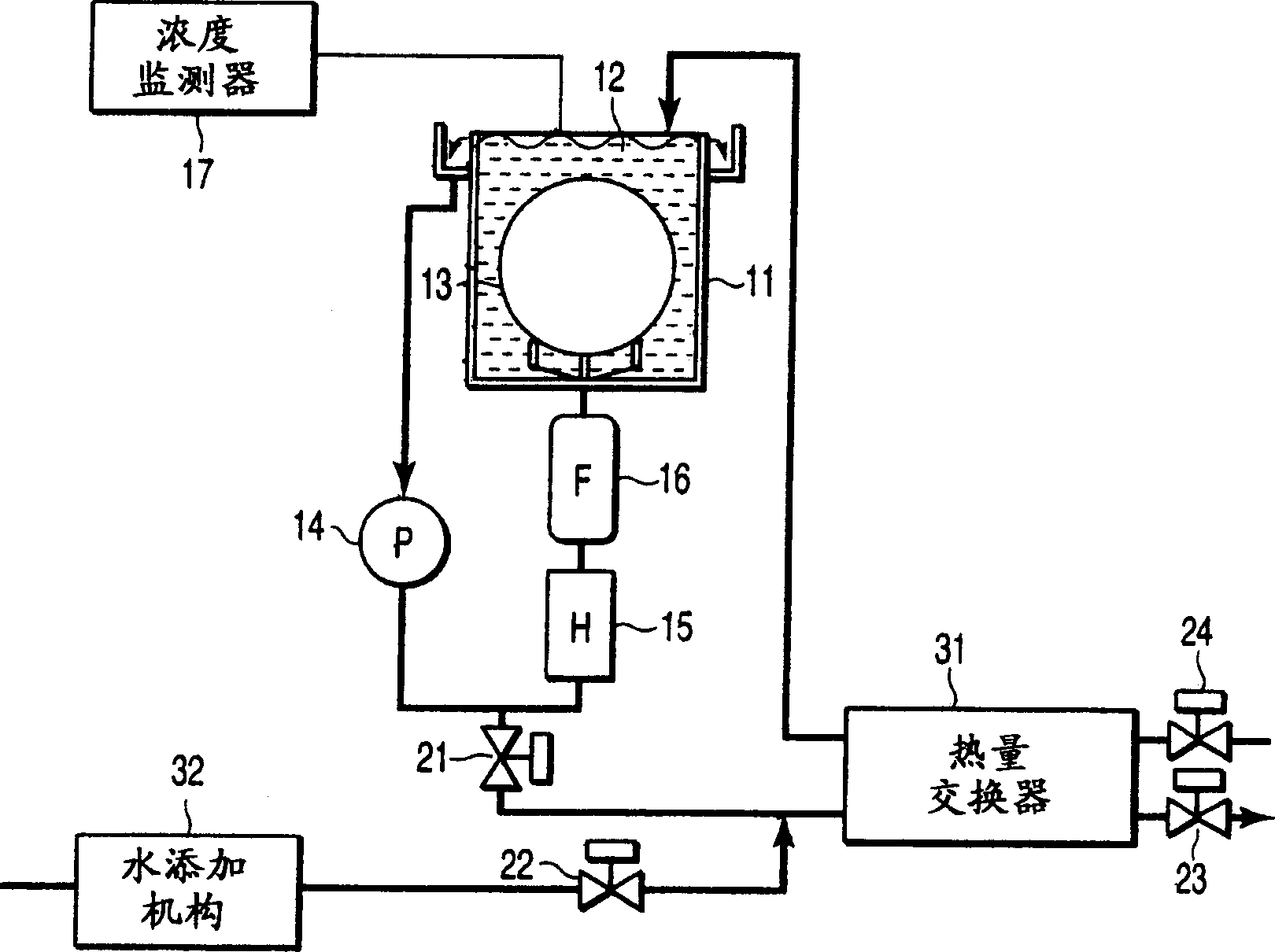
[0019] figure 1 It is a schematic diagram showing a semiconductor manufacturing apparatus according to the first embodiment of the present invention.

[0020] Reference numeral 11 denotes a processing tank (a high-temperature circulation type chemical reagent tank) for cleaning semiconductor substrates such as Si wafers. The treatment tank 11 is filled with, for example, a high-temperature chemical reagent 12 based on sulfuric acid. The semiconductor substrate 13 is immersed in the chemical reagent 12 in the processing tank 11 and then cleaned.

[0021] The chemical reagent 12 in the treatment tank 11 is circulated by the pump (P) 14. That is, the chemical reagent is supplied from the bottom of the processing tank 11 by the pump 14, and the chemical reagent overflowing from the top of the processing tank 11 is supplied again from the bottom of the processing tank 11 through the chemical reagent circuit. A heater (H) 15 that controls the temperature of the chemical reagent and a ...

no. 2 example

[0043] Figure 4 It is a schematic diagram showing a semiconductor manufacturing apparatus according to a second embodiment of the present invention. The same or similar components as those disclosed in the first embodiment are denoted by similar reference numerals and will not be described in detail here.

[0044] The difference between this embodiment and the first embodiment is that the water addition mechanism 32 sets the water addition amount according to the measurement result of the concentration monitor 17. In addition, a valve 25 is provided between the waste chemical reagent valve 21 and the heat exchanger 31. The valve 25 does not allow the waste chemical reagent part to pass through the heat exchanger 31, but allows the waste chemical reagent to be directly discharged. A valve 26 is provided at the new chemical reagent side conduit of the heat exchanger 31, and the valve 26 does not allow the new chemical reagent part to pass through the heat exchanger 31, but allows ...


PUM


Abstract

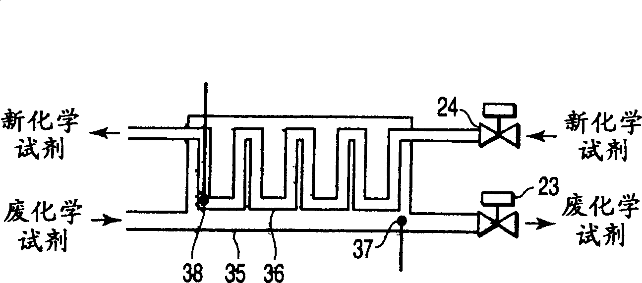
A semiconductor manufacturing device for cleaning a semiconductor substrate is provided with a high temperature circulation-type chemical tank 11 which is filled with a chemical supplied for cleaning the semiconductor substrate in a state that a temperature is raised to a processing temperature, in which the chemical after cleaning is circulated and reused, a bulb 21 discharging the chemical 12 in the chemical tank 11, an auxiliary liquid addition mechanism 32 heating waste liquid by adding auxiliary liquid generating heat by mixing with waste liquid to waste liquid being discharged liquid, a heat exchanger 31 in which heated waste liquid is temporarily stored and new liquid is circulated, waste liquid is cooled and the temperature of new liquid is raised by the heat exchange of waste liquid and new liquid, and piping supplying new liquid whose temperature is raised through the heat exchanger 31 into the chemical tank 11.

Description

Technical field [0001] The invention relates to a semiconductor manufacturing device, in which a high-temperature circulating chemical reagent tank is used to clean a semiconductor substrate, and a chemical reagent exchange method is used to exchange chemical reagents in a high-temperature circulating chemical reagent tank. Background technique [0002] Various methods of cleaning semiconductor substrates have been proposed. When using high-concentration chemical reagents, a system that recycles and cleans the semiconductor substrate with chemical reagents is adopted. In this circulation system, the chemical reagents specially heated for utilization are usually a mixed liquid of sulfuric acid and hydrogen peroxide solution, a mixed liquid of phosphoric acid solution, hydrochloric acid and hydrogen peroxide solution, and a mixed liquid of ammonia water and hydrogen peroxide solution. [0003] In a circulatory system that uses the same chemical reagents to repeatedly clean semicond...

Claims


Application Information

Patent Timeline
Patent Type & Authority Applications(China)
IPC IPC(8): H01L21/00H01L21/306F24J1/00F28D7/10F24V30/00
CPCB08B3/08B08B3/14B08B3/00H01L21/02H01L21/304
Inventor 宫崎邦浩火口隆司中岛俊贵
Owner SEIKO EPSON CORP
Learn More