Organic electroluminescence element
An electroluminescence element and luminescence technology, applied in the direction of electroluminescence light sources, electrical components, electric light sources, etc., can solve problems such as unknown organic EL elements
- Summary
- Abstract
- Description
- Claims
- Application Information
AI Technical Summary
Problems solved by technology
Method used
Image
Examples
Embodiment 1
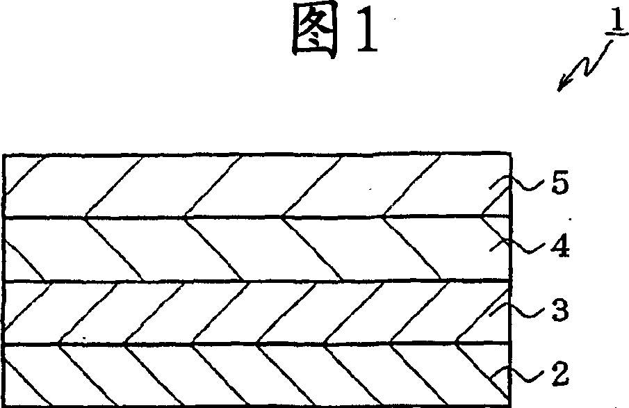
[0276] A 25 mm x 75 mm x 1.1 mm thick glass substrate with an ITO transparent electrode (manufactured by Hoomatik Co., Ltd.) was cleaned ultrasonically for 5 minutes in isopropanol, and then cleaned with UV ozone for 30 minutes.
[0277] Install the cleaned glass substrate with transparent electrode lines on the substrate support of the vacuum evaporation device, and first form a film thickness of 60 nm on the surface of the side where the transparent electrode lines are formed to cover the above-mentioned transparent electrodes. N, N'-bis(N,N'-diphenyl-4-aminophenyl)-N,N-diphenyl-4,4'-diamino-1,1'-biphenyl film (abbreviated below for "TPD232 film"). This TPD232 film functions as a hole injection layer.
[0278] After the TPD232 film is formed, a N,N,N',N'-tetrakis(4-biphenylyl)-diaminobiphenyl layer (hereinafter referred to as "TBDB layer") with a film thickness of 20nm is formed on the TPD232 film . This film functions as a hole transport layer.
[0279] Further, H1 as t...
Embodiment 2
[0285] In addition to making the film thickness of the first light-emitting layer 10 nm and the ratio of D1:H1 to 0.3:10 (weight ratio), the film thickness of the second light-emitting layer was 30 nm and the ratio of D2:H1 to 1.4:30 (weight ratio) Otherwise, an organic EL element was fabricated in exactly the same manner as in Example 1 (about 3.3 mol% of the first dopant and about 5.3 mol% of the second dopant).
Embodiment 3
[0287] In addition to making the film thickness of the first light-emitting layer 20 nm and the ratio of D1:H1 to 0.5:20 (weight ratio), the film thickness of the second light-emitting layer was 20 nm and the ratio of D2:H1 to 1.0:20 (weight ratio) Otherwise, an organic EL element was fabricated in exactly the same manner as in Example 1 (about 2.8 mol% of the first dopant and about 5.7 mol% of the second dopant).
PUM
| Property | Measurement | Unit |
|---|---|---|
| thickness | aaaaa | aaaaa |
| electron work function | aaaaa | aaaaa |
| thickness | aaaaa | aaaaa |
Abstract
Description
Claims
Application Information
 - R&D
- Intellectual Property
- Life Sciences
- Materials
- Tech Scout
- Unparalleled Data Quality
- Higher Quality Content
- 60% Fewer Hallucinations
Browse by: Latest US Patents, China's latest patents, Technical Efficacy Thesaurus, Application Domain, Technology Topic, Popular Technical Reports.
© 2025 PatSnap. All rights reserved.Legal|Privacy policy|Modern Slavery Act Transparency Statement|Sitemap|About US| Contact US: help@patsnap.com


