Capacitor detecting device and its driving method, fingerprint sensor and biological identification device
A detection device, electrostatic capacitance technology, applied in the direction of using electric/magnetic devices to transfer sensing components, electromagnetic measuring devices, measuring devices, etc., can solve problems such as inability to obtain current drive capability, cracking, and transistor size limitations
- Summary
- Abstract
- Description
- Claims
- Application Information
AI Technical Summary
Problems solved by technology
Method used
Image
Examples
no. 1 approach
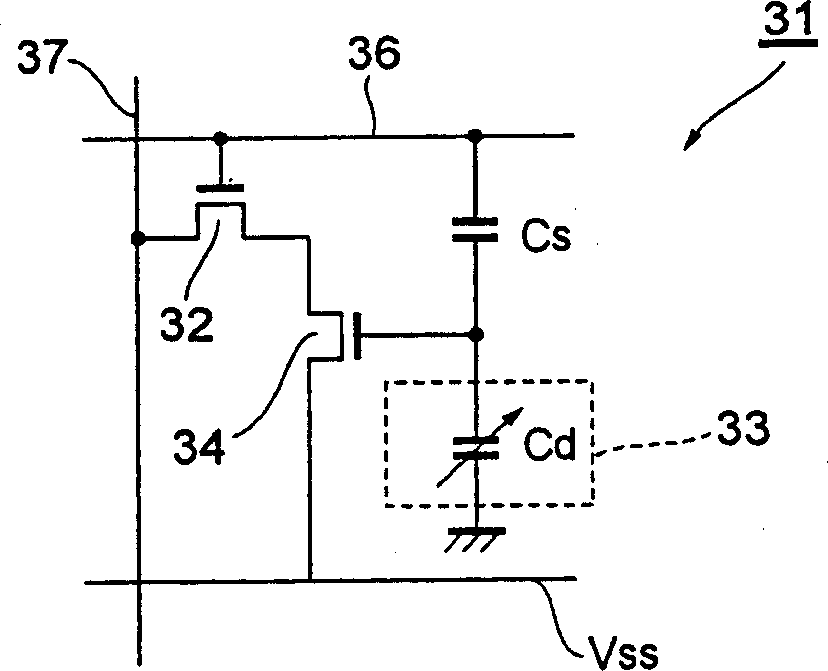
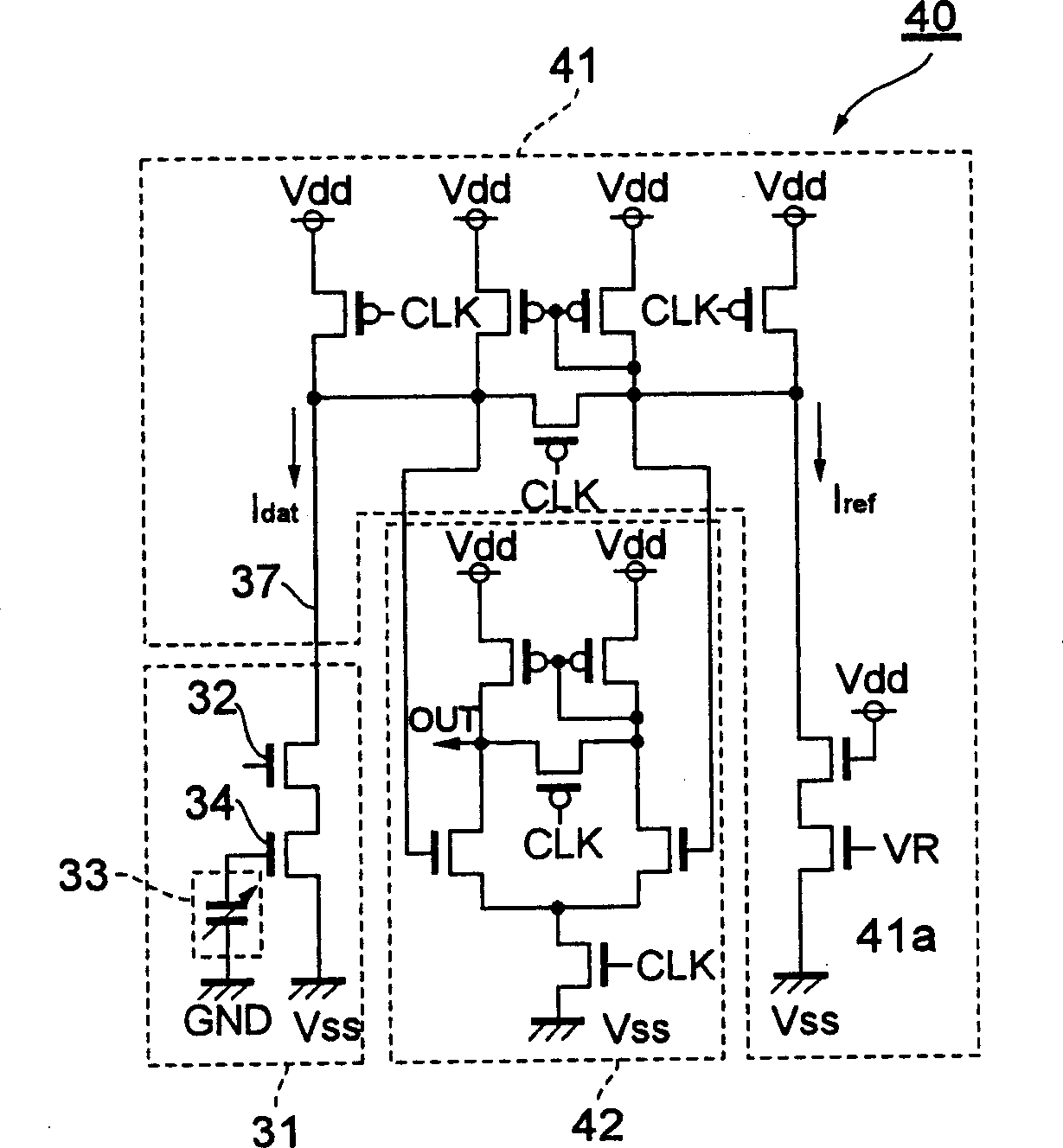
[0035] figure 2 It is a circuit configuration diagram of the electrostatic capacitance detection circuit 31 that converts the unevenness information of the subject's fingerprint into an electrical signal. The detection circuit 31 is configured to include: a selection transistor 32 for selecting the detection circuit 31; an electrostatic capacitance 33 formed between the subject’s finger and the sensor electrode; and a signal output element 34 for a small amount based on the electrostatic capacitance 33 Capacitor to output the detection information with fingerprint concave and convex information; scan line 36 to transmit the signal for switching control of the selection transistor 32; data line 37 to transmit the detection signal; low-potential power supply to form the output path of the detection signal Line Vss; and a reference capacitance Cs with a constant capacitance value. If the capacitance value of the electrostatic capacitance 33 is Cd, the detection capacitance Cd is ba...
Embodiment approach 2
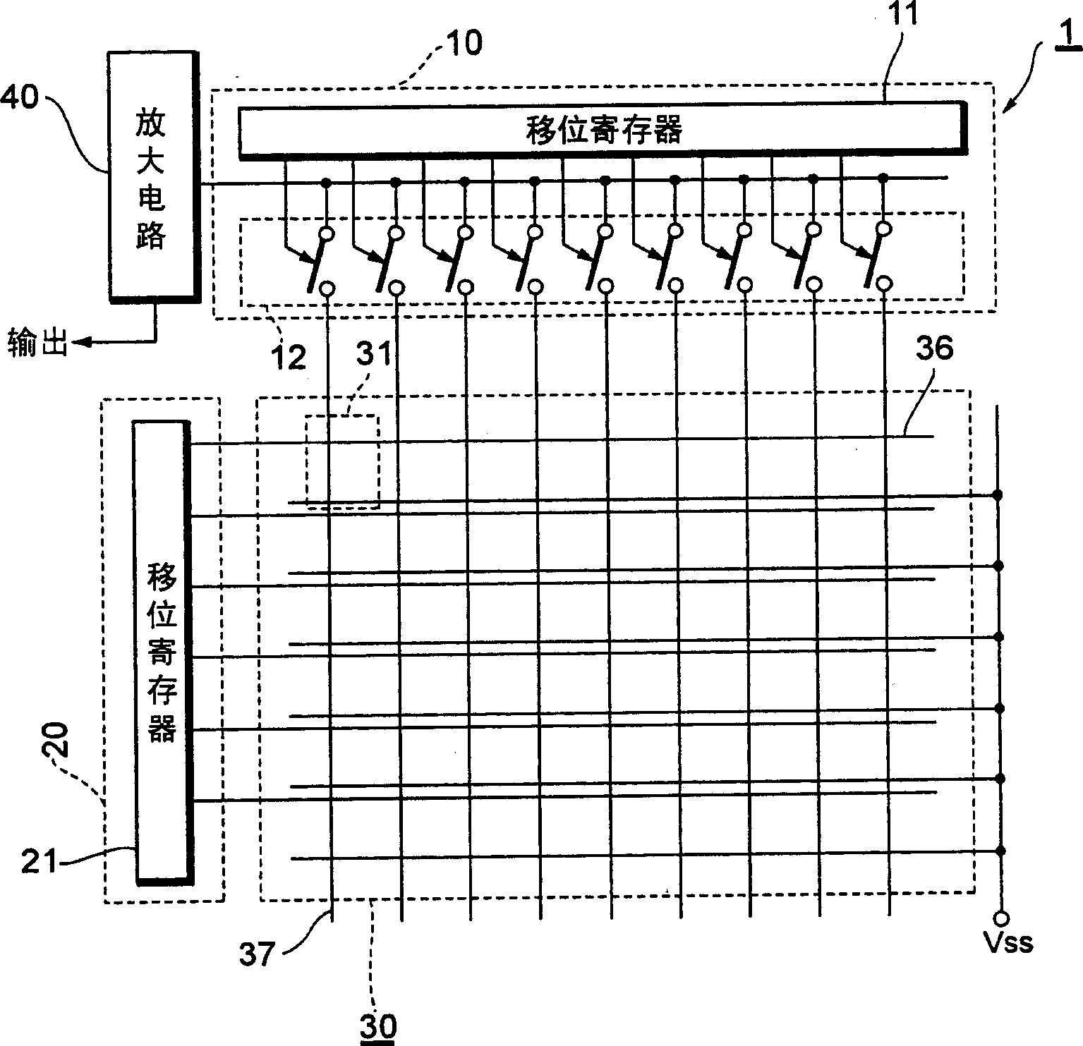
[0050] Figure 7 It is a circuit configuration diagram of the electrostatic capacitance detection circuit 31 of the second embodiment of the present invention. The detection circuit 31 is configured to include the selection transistor 32, the electrostatic capacitor 33, the signal output element 34, the scan line 36, the data line 37, the reference capacitor Cs, and the low-potential power supply line Vss, and the reset transistor 38. The electrostatic capacitance detection circuit 31 shown in the figure is the same as the above-mentioned first embodiment. It is arranged in an array on the active matrix section 30, and the detection of the electrostatic capacitance 33 is read through the control of the data line driver 10 and the scan line driver 20. Capacity Cd. The reset transistor 38 is switched and controlled to be turned on during the stage (presensing time) of selecting the previous-stage electrostatic capacitance detection circuit 31.
[0051] Since the reset transistor 38...
Embodiment approach 3
[0054] Picture 9 It is a circuit configuration diagram of the electrostatic capacitance detection circuit 31 of the third embodiment of the present invention. The detection circuit 31 is configured to include the selection transistor 32, the electrostatic capacitor 33, the signal output element 34, the scanning line 36, the data line 37, the reference capacitor Cs, and the low-potential power supply line Vss, as well as the data line selection transistor 35, Line 50 is selected on the data side. The electrostatic capacitance detection circuit 31 shown in the figure is the same as the above-mentioned first embodiment. It is arranged in the active matrix section 30 in M rows×N columns, and is read by the control of the data line driver 10 and the scan line driver 20. The detection capacity Cd of the electrostatic capacitor 33.
[0055] Focus on a specific data line 37. Since the detection signals from the M electrostatic capacitance detection circuits 31 arranged in the column d...
PUM
 Abstract
Description
Claims
Application Information
 - Generate Ideas
- Intellectual Property
- Life Sciences
- Materials
- Tech Scout
- Unparalleled Data Quality
- Higher Quality Content
- 60% Fewer Hallucinations
Browse by: Latest US Patents, China's latest patents, Technical Efficacy Thesaurus, Application Domain, Technology Topic, Popular Technical Reports.
© 2025 PatSnap. All rights reserved.Legal|Privacy policy|Modern Slavery Act Transparency Statement|Sitemap|About US| Contact US: help@patsnap.com


