


Quick Research
Generate reliable direction feasibility study reports for your R&D in just a few steps.

Technical Q&A
Discover and master advanced knowledge NOW. Basics, ideas, possibilities, all at once.

Find Solutions
As an expert in R&D theories, this can generate solutions to your technical problems instantly.

Evaluate Feasibility
Analyze your overall solution with one click, know your potential R&D risks in advance.

Monitor Landscape
Get weekly tech updates, stay abreast of the latest tech innovations and key insights.
Solid camera device, driving method thereof and camera
A technology of solid-state photography and motion, applied in the field of solid-state photography devices and cameras, can solve problems such as long-term and achieve the effect of not sacrificing sensitivity
- Summary
- Abstract
- Description
- Claims
- Application Information
AI Technical Summary
Problems solved by technology
Method used
Image

Examples
Embodiment approach 1
[0140] In Embodiment 1, a CCD (charge-coupled device) sensor of a progressive scanning method will be described as a solid-state imaging device.
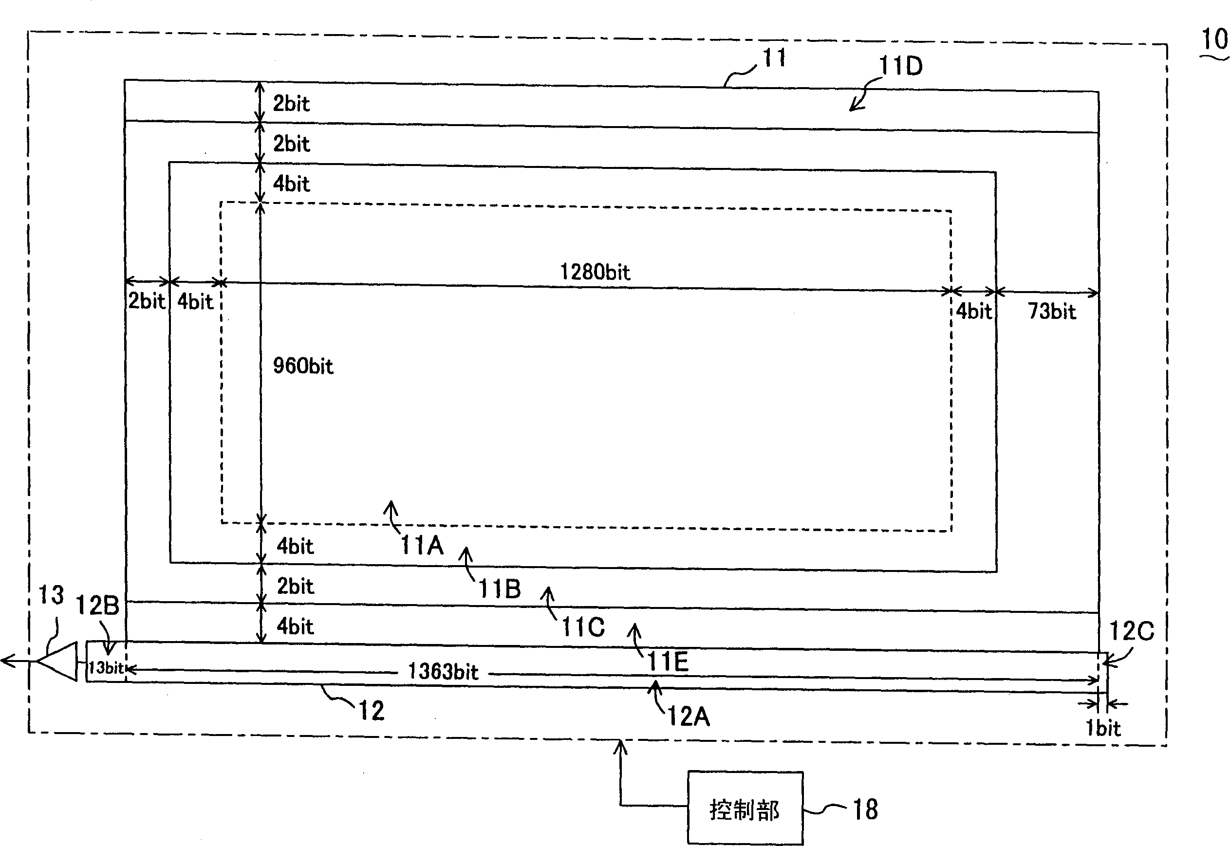
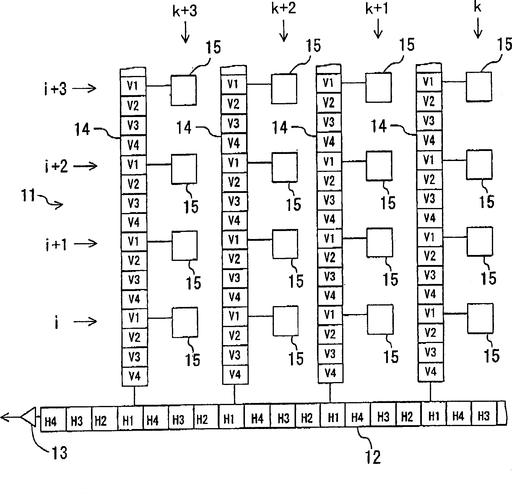
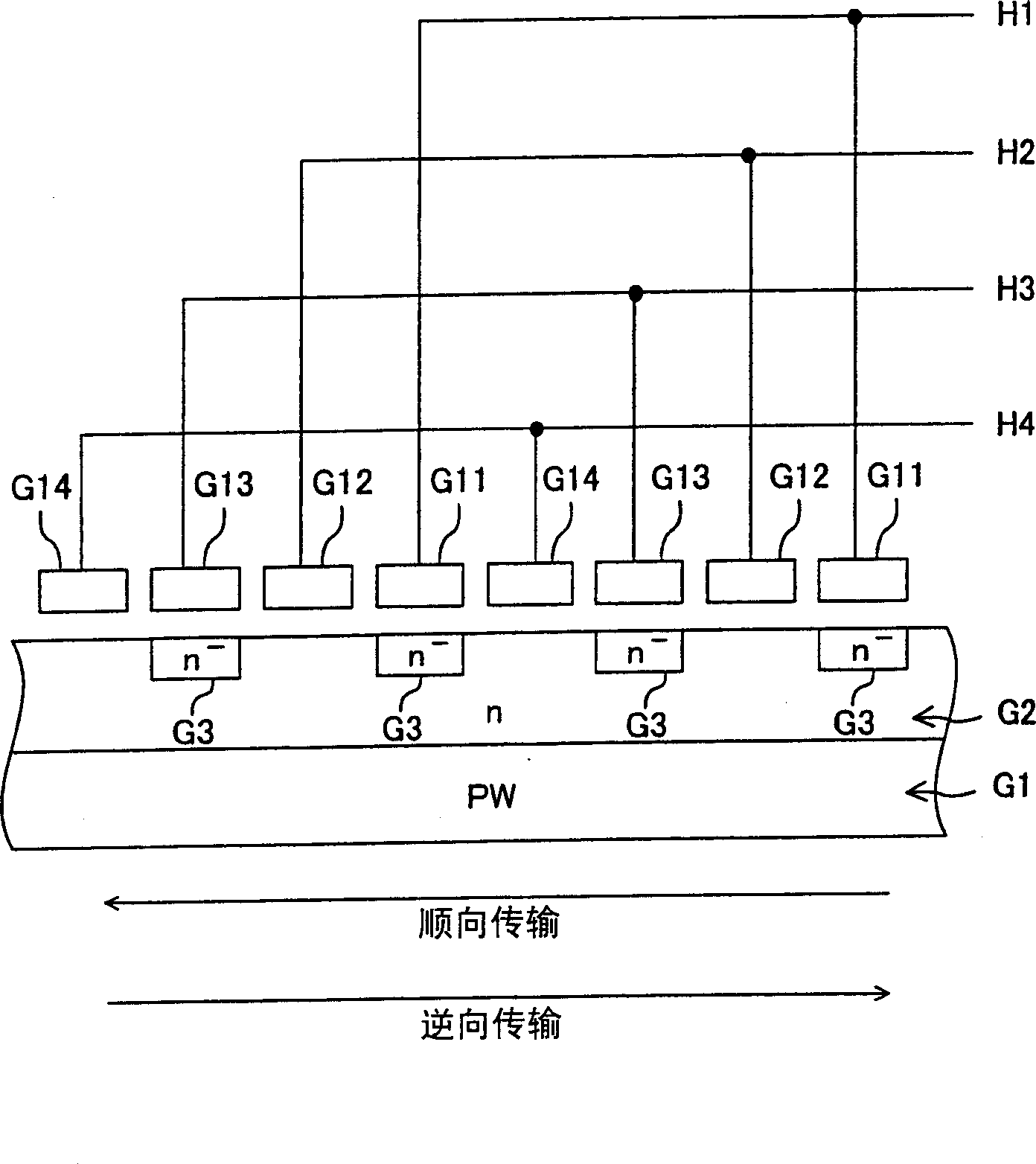
[0141] figure 1 It is an explanatory diagram showing a configuration example of the CCD sensor 10 according to Embodiment 1 of the present invention. figure 1 The CCD sensor 10 has a pixel section 11, a horizontal transfer section 12, a charge detection section 13, a vertical transfer section ( figure 1 not shown) and the control unit 18. In addition, this CCD sensor 10 employs a simultaneous independent readout method for all pixels.
[0142] The pixel portion 11 has an effective pixel area 11A, a transient area 11B, a shadow area 11C, and vertical empty areas 11D and 11E. The effective pixel area 11A has 1280 (horizontal)×960 (vertical) photodiodes as photoelectric change elements arranged in a matrix. One photodiode constitutes one pixel. Here, the array of pixels in the horizontal direction is called a row, and the array...
Embodiment approach 2
[0216] In Embodiment 2, a CCD sensor of an interlaced scanning method will be described as a solid-state imaging device.
[0217] Figure 17 It is an explanatory diagram showing a configuration example of the CCD sensor 30 according to Embodiment 2 of the present invention. Figure 17 The CCD sensor 30 has a pixel portion 31, a horizontal transfer portion 32, a charge detection portion 33, a vertical transfer portion ( Figure 17 Not shown in ) and the control unit 38.
[0218] The pixel section 31 has an effective pixel area 31A, a momentary area 31B, a shadow area 31C, and vertical empty areas 31D and 31E. The effective pixel area 31A has 1280 (horizontal)×960 (vertical) photodiodes as photoelectric conversion elements arranged in a matrix. One photodiode constitutes one pixel. Each of the regions 31A to 31E of the pixel portion 31 and figure 1 Each of the regions 11A to 11E of the pixel unit 11 of the CCD sensor 10 has the same arrangement and the same number of pixel...
Embodiment approach 3
[0258] In Embodiment 3, a MOS (metal oxide semiconductor) sensor, particularly a CMOS (complementary MOS) sensor will be described as a solid-state imaging device.
[0259] Figure 27 It is a block diagram showing a configuration example of the CMOS sensor 50 according to Embodiment 3 of the present invention. Figure 27 The CMOS sensor 50 has a pixel address specifying circuit 312, a control section 314, a synchronization signal generator 316, a timing generator 318, a vertical register (row address selection section) 322, a latch array 324, a horizontal register (column address selection section) 326 , a sense amplifier 328 and a pixel unit 340 .
[0260] The pixel unit 340 has an empty area 342 , an effective pixel area 344 , a light and shadow area 346 , and an empty transfer area 348 . The effective pixel area 344 has 1280 (horizontal)×960 (vertical) photodiodes as photoelectric conversion elements arranged in a matrix. One photodiode constitutes one pixel.
[0261] F...
PUM
 Abstract
Description
Claims
Application Information
 - R&D Engineer
- R&D Manager
- IP Professional
- Industry Leading Data Capabilities
- Powerful AI technology
- Patent DNA Extraction
Browse by: Latest US Patents, China's latest patents, Technical Efficacy Thesaurus, Application Domain, Technology Topic, Popular Technical Reports.
© 2024 PatSnap. All rights reserved.Legal|Privacy policy|Modern Slavery Act Transparency Statement|Sitemap|About US| Contact US: help@patsnap.com