Flip-flop circuit
A technology of triggers and circuits, applied in electrical components, generating electrical pulses, pulses, etc., to prevent unnecessary changes, reduce power consumption, and reduce the number of
- Summary
- Abstract
- Description
- Claims
- Application Information
AI Technical Summary
Problems solved by technology
Method used
Image
Examples
no. 1 Embodiment
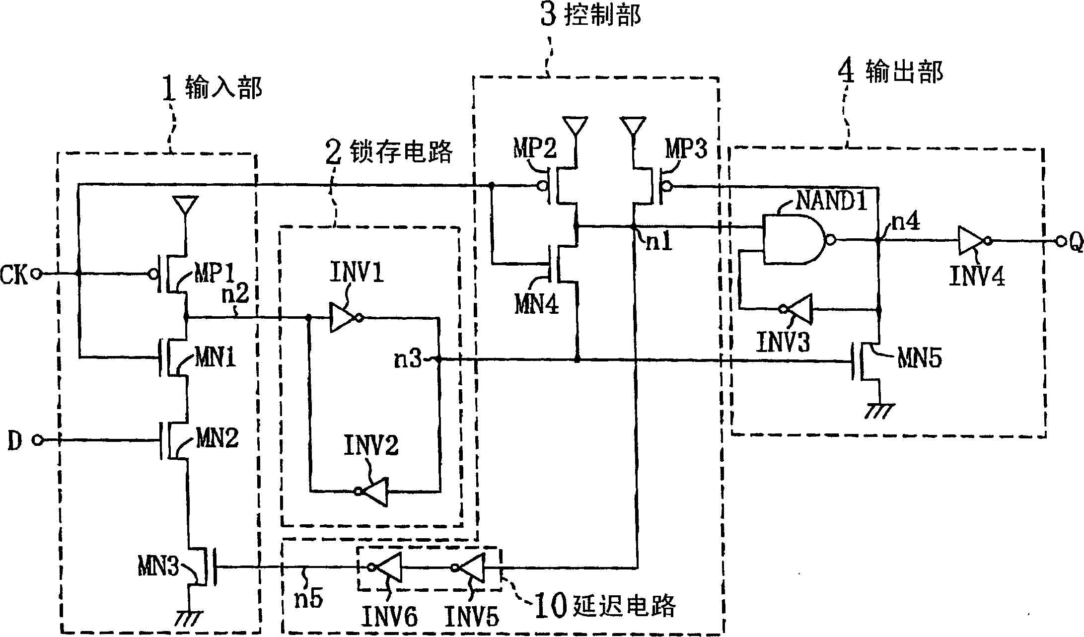
[0054] figure 1 A circuit diagram showing a flip-flop circuit in the first embodiment of the present invention. In the figure, D denotes an input terminal, CK denotes a clock terminal, and Q denotes an output terminal. 1 denotes a dynamic type input part, 2 denotes a latch circuit, 3 denotes a control part, and 4 denotes a static type output part.
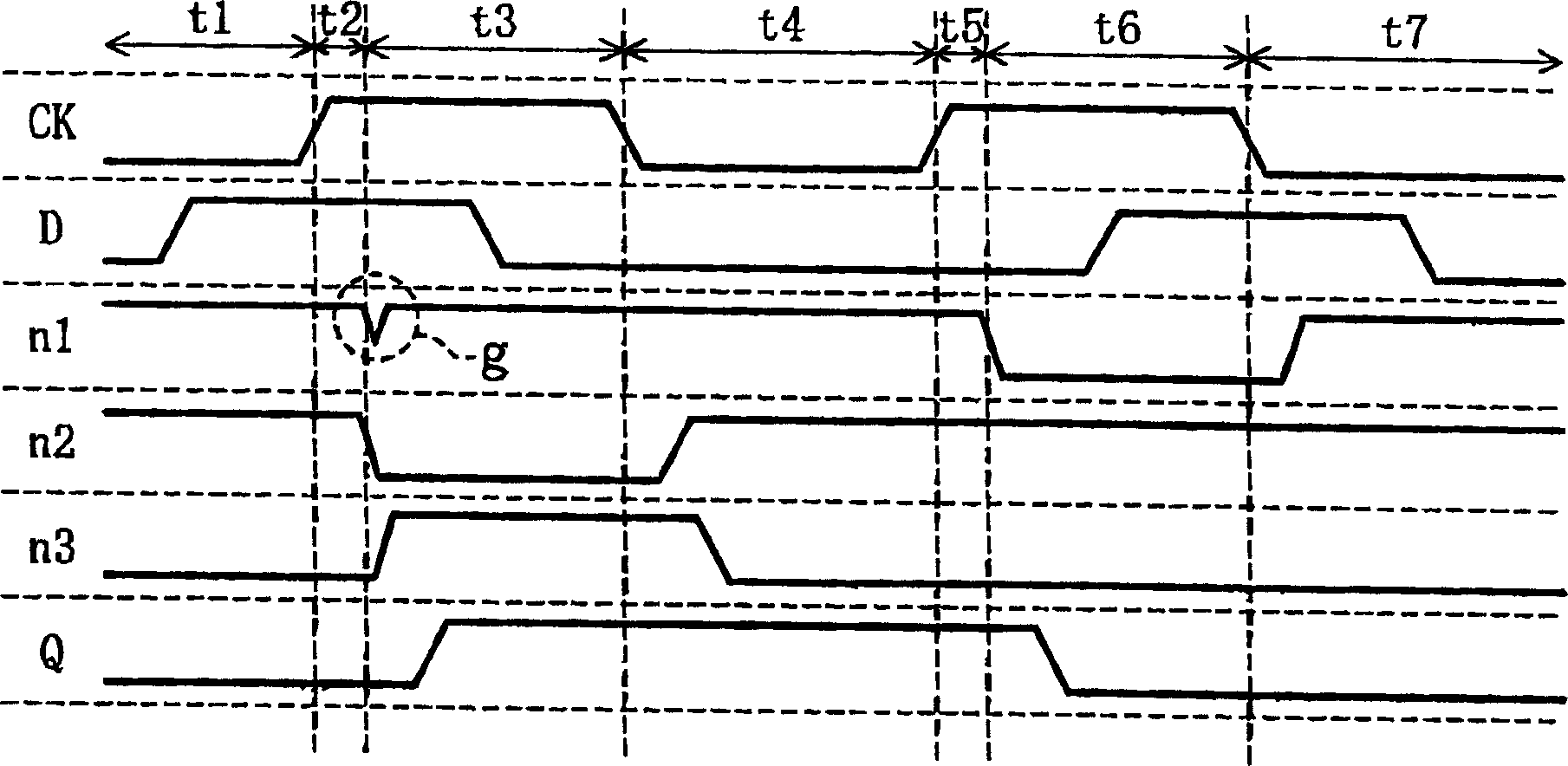
[0055]The control unit 3 has a first node n1, and controls the operation of the input unit 1 using a signal of the first node n1 as a control signal. The input unit 1 receives a clock signal from the clock terminal CK (hereinafter simply referred to as the clock signal CK) and an input signal from the input terminal D (hereinafter referred to as the input signal D), and has a second node n2 from which n2 output signal. The latch circuit 2 receives an output signal from the second node n2 of the input unit 1, has a third node n3, latches the output signal from the input unit 1, and outputs a latch signal from the third node n3. ...
no. 2 Embodiment
[0074] Refer to the following image 3 A flip-flop circuit according to a second embodiment of the present invention will be described. In addition, in the following embodiments, components having the same functions as those in the first embodiment described above are denoted by the same reference numerals, and description thereof will be omitted.
[0075] image 3 The flip-flop circuit shown and described in the first embodiment above figure 1 The circuits of 1 and 2 have substantially the same configuration, and the difference is that a delay circuit 10 is added to the control unit 3 . which is, image 3 In order to delay the control signal applied from the first node n1 to the gate of the NMOS transistor MN3 of the input unit 1, the control signal at the first node n1 is delayed by two inverter circuits INV5 and INV6 connected in series. The circuit 10 is then applied to the gate of the NMOS transistor MN3 of the input section 1 . Here, the connection point between th...
no. 3 Embodiment
[0080] A flip-flop circuit according to a third embodiment of the present invention will be described below with reference to the drawings.
[0081] Figure 4 A circuit diagram showing a flip-flop circuit of this embodiment. basic composition and image 3 The flip-flop circuit shown is the same. In this example Figure 4 circuit, just put the image 3 The arrangement position of the PMOS transistor MP3 in the second embodiment shown is changed. That is, in image 3 The middle gate is connected to the fourth node n4 and is connected to the PMOS transistor MP3 between the power supply and the first node n1. In this embodiment, the gate is connected to the second node n2 of the input part 1 and is connected in parallel with the NMOS transistor MN4. connection for pulling up the first node n1 to the power supply potential.
[0082] In this example Figure 4 of the flip-flop circuit, the hold image 3 In the case of the function of the flip-flop circuit in , when the input...
PUM
 Abstract
Description
Claims
Application Information
 - R&D Engineer
- R&D Manager
- IP Professional
- Industry Leading Data Capabilities
- Powerful AI technology
- Patent DNA Extraction
Browse by: Latest US Patents, China's latest patents, Technical Efficacy Thesaurus, Application Domain, Technology Topic, Popular Technical Reports.
© 2024 PatSnap. All rights reserved.Legal|Privacy policy|Modern Slavery Act Transparency Statement|Sitemap|About US| Contact US: help@patsnap.com


