Semiconductor laser device
A laser device and semiconductor technology, which is applied to the structure of semiconductor lasers, lasers, and optical waveguide semiconductors, can solve problems such as increased resistance and reduced light output, and achieve the effects of reduced light absorption and improved slope efficiency
- Summary
- Abstract
- Description
- Claims
- Application Information
AI Technical Summary
Problems solved by technology
Method used
Image


Examples
Embodiment 1
[0035] FIG. 1 is a cross-sectional view of a semiconductor laser according to Embodiment 1 of the present invention.
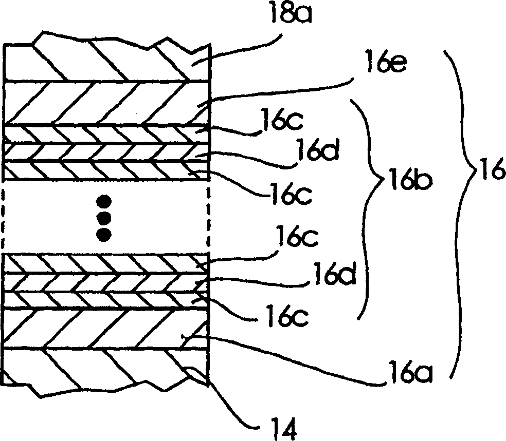
[0036] In FIG. 1 , 10 denotes a semiconductor laser, and in the cross section of the semiconductor laser 10 in FIG. 1 , the direction perpendicular to the paper is the waveguide direction. 12 represents the p-InP substrate as the semiconductor substrate, and 14 represents the p-InP cladding layer as the first cladding layer arranged on the p-InP substrate 12, and the bandgap energy of this p-InP cladding layer 14 is 1.35eV, the layer thickness is 1000nm, and the carrier concentration is 1×10 18 cm -1 . 16 denotes an active region provided on the p-InP cladding layer 14 .
[0037] 18 represents the n-InP cladding layer as the second cladding layer provided on the active region 16. This n-InP cladding layer 18 is divided into two layers in this embodiment 1, and the n-InP cladding layer adjacent to the active region 16 The cladding layer 18a is composed of a...
Embodiment 2
[0085] Fig. 8 is a cross-sectional view of a semiconductor laser according to Embodiment 2 of the present invention.
[0086] In FIG. 8 , 40 denotes a semiconductor laser, and in the cross section of the semiconductor laser 40 in FIG. 8 , the direction perpendicular to the paper surface is the waveguide direction. 42 denotes a p-AlGaInAs cladding layer as a semiconductor layer.
[0087] Because semiconductor laser 40 adopts p-InP substrate 12, structure is roughly the same as semiconductor laser 10 of embodiment 1, but, be provided with its refractive index ratio n-InP cladding 18 in n-InP cladding 18 for semiconductor laser 10 High n-InGaAsP cladding layer 20, and in semiconductor laser 40, p-AlGaInAs cladding layer whose refractive index is lower than p-InP cladding layer 14 is inserted in p-InP cladding layer 14.
[0088] In the semiconductor laser 40, the p-AlGaInAs cladding layer 42 is interposed between the p-InP cladding layer 14d and the p-InP cladding layer 14c.
[...
Embodiment 3
[0109] Fig. 11 is a cross-sectional view of a semiconductor laser according to Embodiment 3 of the present invention.
[0110] In FIG. 11 , 50 denotes a semiconductor laser, and in the cross section of the semiconductor laser 50 in FIG. 11 , the direction perpendicular to the paper surface is the waveguide direction.
[0111] 52 represents an n-InP substrate as a semiconductor substrate, an n-InP cladding layer 18b is set on the n-InP substrate 52, an n-InGaAsP cladding layer 20 is set on the n-InP cladding layer 18b, and then - An n-InP cladding layer 18 a is provided on the InGaAsP cladding layer 20 . The n-InP cladding layer 18a and the n-InP cladding layer 18b constitute the n-InP cladding layer 18 as the first cladding layer.
[0112] Furthermore, the active region 16 is provided on the n-InP cladding layer 18a, and the p-InP cladding layer 14 as a second cladding layer is provided on the active region 16.
[0113] The ridge shape is formed by the p-InP cladding layer 1...
PUM
 Abstract
Description
Claims
Application Information
 - R&D
- Intellectual Property
- Life Sciences
- Materials
- Tech Scout
- Unparalleled Data Quality
- Higher Quality Content
- 60% Fewer Hallucinations
Browse by: Latest US Patents, China's latest patents, Technical Efficacy Thesaurus, Application Domain, Technology Topic, Popular Technical Reports.
© 2025 PatSnap. All rights reserved.Legal|Privacy policy|Modern Slavery Act Transparency Statement|Sitemap|About US| Contact US: help@patsnap.com