Delay phase-locking loop unit and its clock signal generating method

A technology of delay-locked loop and clock signal, which is applied to the automatic control of power and electrical components, etc. It can solve the problems of data reception error at the receiving end, signal delay accuracy and insufficient transmission rate, etc.

Inactive Publication Date: 2003-03-19
VIA TECH INC
View PDF0 Cites 6 Cited by
  • Summary
  • Abstract
  • Description
  • Claims
  • Application Information

AI Technical Summary

Problems solved by technology

[0004] Since the count value received by each controlled delay line in the controlled delay circuit 21 is the same, it can be ensured that the phases of the four output clock signals can be evenly distributed and have a difference of 90 degrees every two, but this method is different from each time The adjustment action will change a total of 4 delay units. Therefore, the lack of accuracy of the signal delay will cause serious problems when the transmission rate is increased in the future.
In addition, common means can only ensure that the formed parallel data signal (TX_D) is in an ideal state at the source 101, because after these signals are sent out by the source 101, they need to go through different transmission paths to reach the I / O pad group (I / OPad). )102
And because different transmission paths will produce different degrees of delay effect (skew) and interference to these signals, the strobe signal (strobe) and the parallel data signal output by the I / O pad group (I / O Pad) 102 will be The waveform shown in Figure 2(c) may be generated, for example, the rising and falling edges of the strobe signal may not be generated in the middle of the parallel data signal (TX_D)
This may cause data receiving errors at the receiving end of the memory module 11, and this situation will become more serious when the transmission rate is increased. How to improve this defect is the main purpose of the present invention

Method used


Image

  • Delay phase-locking loop unit and its clock signal generating method
  • Delay phase-locking loop unit and its clock signal generating method
  • Delay phase-locking loop unit and its clock signal generating method

Examples


Embodiment Construction

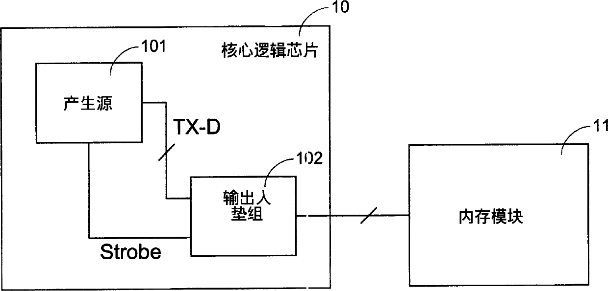
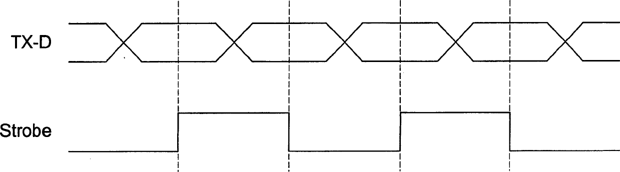
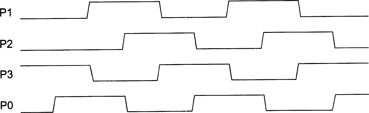
[0028] Please refer to FIG. 3 , which is a schematic block diagram of a preferred embodiment of the present invention developed to improve common defects. The improved delay-locked loop device (Delay-Locked Loop, DLL) also receives a reference clock signal CLK and sends it to into a controlled delay circuit 31 for phase delay processing. The controlled delay circuit 31 is also formed by connecting four controlled delay lines (delay lines) 311, 312, 313, 314, and each controlled delay line is mainly composed of several delay units (delay units) ( not shown in the figure). After the reference clock signal CLK passes through the four controlled delay lines 311 , 312 , 313 , and 314 , it can basically generate four output clock signals P1 , P2 , P3 , and P0 with different phases.

[0029] Similarly, in order to keep the state in phase with the reference clock signal CLK, the output clock signal P0 and the reference clock signal CLK are simultaneously input to a phase detector 32 ...


PUM


Abstract

The delay phase-locking loop unit is used to receive a reference clock signal and produce several output clock signals in different phases. It includes one controlled delay circuit, one phase monitor and one control circuit. The production of clock signal includes the following steps: receiving one reference clock signal; phase delaying in the controlled delay circuit and outputting several output clock signals in different phases. The control circuit outputs one regulating signal corresponding to the phase difference between the output clock signal and the reference clock signal; and the controlled delay circuit delays the output signal corresponding to the control signal.

Description

technical field [0001] The invention relates to a delay-locked loop device and a clock signal generating method, in particular to a delay-locked loop device and a clock signal generating method applied in a core logic circuit chip. Background technique [0002] In the personal computer architecture, apart from the central processing unit, the components that most affect the data processing performance are the core logic chip and the memory module. Please refer to FIG. 1(a), which is a functional block diagram of a core logic chip 10 connected to a memory module 11. Under the double data transfer rate (DDR) specification, when the core logic chip 10 is to parallel a When data is transmitted to the memory module 11, the core logic chip 10 needs to transmit a strobe signal (strobe) together with a parallel data signal (TX_D) to the memory module 11 outside the chip, and then provide the memory module 11 to read data When used, please refer to Figure 1(b) for the ideal waveform...

Claims


Application Information

Patent Timeline
Patent Type & Authority Applications(China)
IPC IPC(8): H03L7/081H03L7/089
CPCH03L7/0814H03L7/089H03L7/0816
Inventor 何桓蓁
Owner VIA TECH INC
Why Eureka
Try Eureka