Semiconductor storage equipment and electronic information equipment using said device

A storage device and semiconductor technology, applied in the direction of digital memory information, static memory, read-only memory, etc., can solve the problem of changing the clock cycle

Inactive Publication Date: 2007-07-18
泰拉曼第九基金会有限责任公司
View PDF3 Cites 0 Cited by
  • Summary
  • Abstract
  • Description
  • Claims
  • Application Information

AI Technical Summary

Problems solved by technology

[0059] Therefore, the microprocessor technology disclosed by Japanese Laid-Open Publication No. 8-161286 cannot be used to change the clock period according to whether an application operation is performed or a voltage increase or decrease operation is performed.
It also cannot be used to change the clock period depending on whether the latch registers A to C close to the processing circuit 101 or the latch registers D to F far from the processing circuit 101 are to be accessed

Method used


Image

  • Semiconductor storage equipment and electronic information equipment using said device
  • Semiconductor storage equipment and electronic information equipment using said device
  • Semiconductor storage equipment and electronic information equipment using said device

Examples


example 1

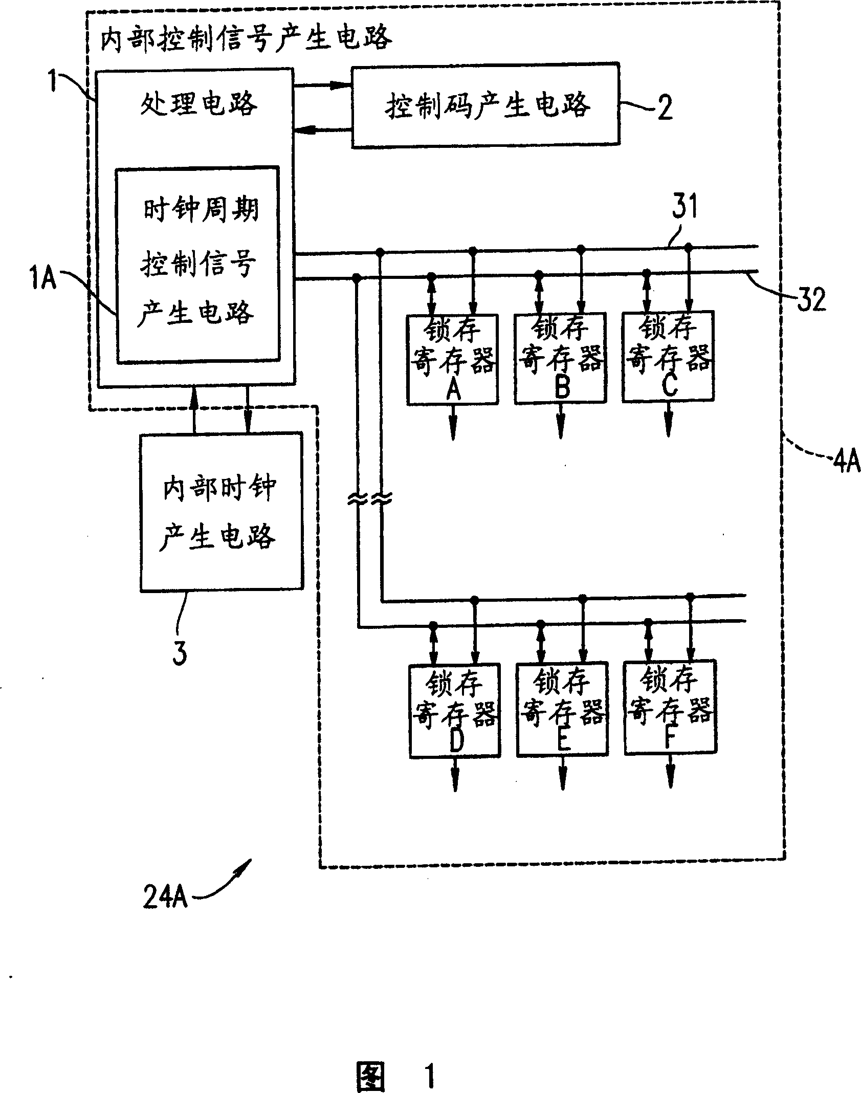
[0101] FIG. 1 is a partial block diagram of a write state machine 24A included in a flash memory according to a first example of the present invention.

[0102] As shown in FIG. 1, the write state machine 24A includes: a processing circuit 1 that executes different processing types, a control code generation circuit 2 that provides control codes to the processing circuit 1, and a timing signal (internal clock signal) that provides the processing circuit 1. The internal clock generating circuit 3, and a plurality of latch registers A-F (latch section) connected to the processing circuit 1. As described in detail below, the write state machine 24A can be based on the storage operation included in writing data to the memory cell or erasing data from the memory cell (that is: the operation of raising the internal voltage, the operation of applying the write voltage or the erase voltage, and The operation time characteristic of each of the operations of lowering the internal voltag...

example 2

[0133] In the first example, the internal control signal generating circuit 4A includes a clock cycle control signal generating section 1A for supplying the clock cycle control signal to the internal clock generating circuit 3 as an internal control for changing the clock cycle Signal. In the second example, the internal control signal generation circuit 4B includes a clock period control signal latch section 5B for supplying the clock period control signal to the internal clock generation circuit 3 as a change Internal control signal for clock cycles.

[0134] FIG. 6 is a partial block diagram of a write state machine 24B included in a flash memory according to a second example of the present invention.

[0135] As shown in Figure 6, the write state machine 24B includes: a processing circuit 1 that performs different types of processing, a control code generation circuit 2 that provides control codes to the processing circuit 1, and a timing signal (internal clock signal) th...


PUM


Abstract

In a semiconductor memory device for performing a memory operation by controlling an internal voltage and a memory operation voltage, a cycle of an internal clock signal is varied in accordance with operation time characteristics of the memory operation.

Description

technical field [0001] The present invention relates to a semiconductor storage device, such as a flash memory, used in an electronic information device such as a cellular phone, and to an electronic information device using such a semiconductor storage device. Background technique [0002] In general, a flash memory performs operations such as data writing or data erasing by controlling the operation of raising or lowering an internal voltage and controlling the operation of applying a pulse voltage for writing information to or erasing information from a memory cell. storage operations. This control is performed in synchronization with an internal clock signal generated in the control circuit. [0003] Fig. 9 shows a partial structural block diagram of a conventional conventional flash memory. [0004] As shown in FIG. 9, the flash memory includes a memory array 11 having a plurality of memory cells (not shown) arranged in row and column directions. These memory cells a...

Claims


Application Information

Patent Timeline
Patent Type & Authority Patents(China)
IPC IPC(8): G11C11/34G11C11/4063G11C7/00G11C16/02G11C7/22G11C16/32
CPCG11C16/32G11C2207/2227G11C7/222G11C7/22
Inventor 木曾弘志
Owner 泰拉曼第九基金会有限责任公司
Why Eureka
Try Eureka