Stacked photovoltaic element
A photoelectric element, stacked technology, applied in the field of solar cells, can solve problems such as inability to effectively implement photoelectric conversion, difficult to manage film thickness, and spectral sensitivity spectrum without wavelength selectivity
- Summary
- Abstract
- Description
- Claims
- Application Information
AI Technical Summary
Problems solved by technology
Method used
Image

Examples
Embodiment 1
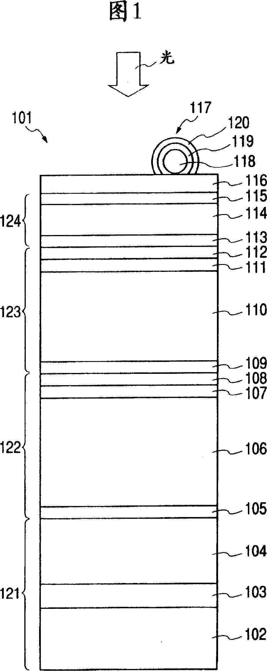
[0074] This example is an example in which the photoelectric element of FIG. 1 was produced. First, the substrate of the photovoltaic element of the present invention was fabricated using the apparatus shown in FIGS. 9 and 10 .
[0075] The device 301 in FIG. 9 is a roll-to-roll type film forming device, and can simultaneously and continuously form different films in different spaces on the belt-shaped support 302 . 303, 304, and 305 are vacuum chambers for forming thin films by DC sputtering, and the formed thin films can be changed by changing the target material. Using a Ti target in the vacuum chamber 303, an Ag target in 304, and a ZnO target in 305, a Ti layer, an Ag layer, and a ZnO layer can be sequentially formed on the support.
[0076] Inside each vacuum chamber, there is a heater 310 for heating the strip-shaped support 302 from the back surface, and the strip-shaped support 302 is sandwiched, and a target 311 and an electrode 312 connected to the target are provi...
Embodiment 2
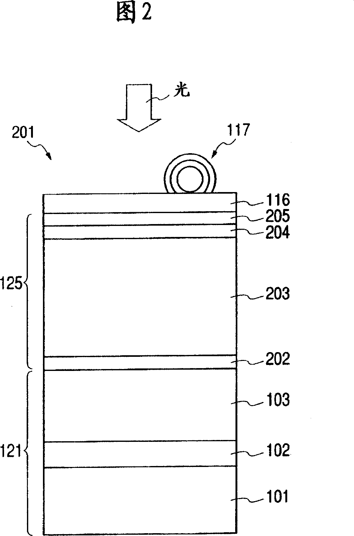
[0107] The same photovoltaic element as in Example 1 was formed except that a 2.8 μm ZnO layer by sputtering was used as a substrate instead of forming a ZnO layer by an electrolytic method as the lower transparent conductive layer 104 . As a result, it was found that, similarly to Example 1, good characteristics and yield were obtained.
Embodiment 3
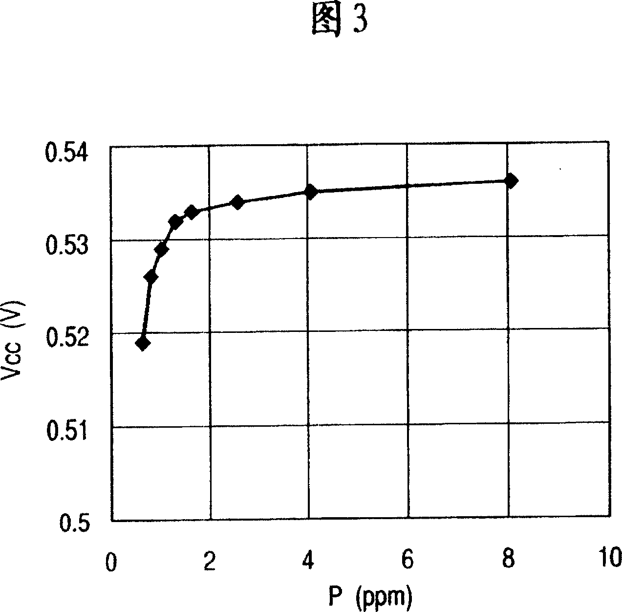
[0109] In addition to the pH of 0.01 sccm flowing through the vacuum chamber 503 during the formation of the Type I layer of the bottom unit of Example 1 3 Except for the gas, the same photovoltaic element as in Example 1 was fabricated. As a result, it was found that, similarly to Example 1, good characteristics and yield were obtained.
[0110] In this way, according to the multilayer photoelectric element and the current balance adjustment method of the embodiment of the present invention, it is possible to manufacture a photoelectric element with high conversion efficiency at a high yield.
PUM
 Abstract
Description
Claims
Application Information
 - R&D
- Intellectual Property
- Life Sciences
- Materials
- Tech Scout
- Unparalleled Data Quality
- Higher Quality Content
- 60% Fewer Hallucinations
Browse by: Latest US Patents, China's latest patents, Technical Efficacy Thesaurus, Application Domain, Technology Topic, Popular Technical Reports.
© 2025 PatSnap. All rights reserved.Legal|Privacy policy|Modern Slavery Act Transparency Statement|Sitemap|About US| Contact US: help@patsnap.com