Hv-SOI LDMOS device with integrated diode to improve reliability and avalanche ruggedness

A diode and device technology, applied in the field of lateral drift metal oxide semiconductor devices, can solve problems such as destroying devices and semiconductor device breakdown

Inactive Publication Date: 2007-02-28
NXP BV
View PDF4 Cites 0 Cited by
  • Summary
  • Abstract
  • Description
  • Claims
  • Application Information

AI Technical Summary

Problems solved by technology

[0005] For example, when used for lighting, the typical drain-to-source voltage is 400V. If the impact of this voltage reaches 500V or higher, the sem...

Method used


Image

  • Hv-SOI LDMOS device with integrated diode to improve reliability and avalanche ruggedness
  • Hv-SOI LDMOS device with integrated diode to improve reliability and avalanche ruggedness
  • Hv-SOI LDMOS device with integrated diode to improve reliability and avalanche ruggedness

Examples


Embodiment Construction

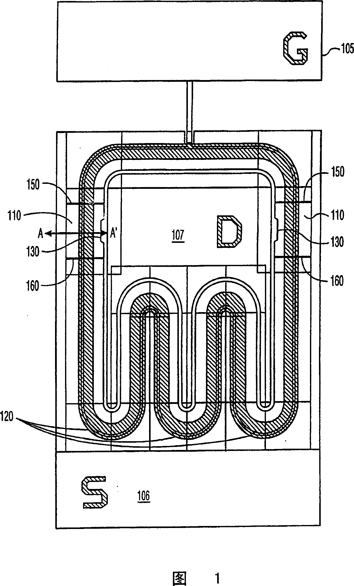
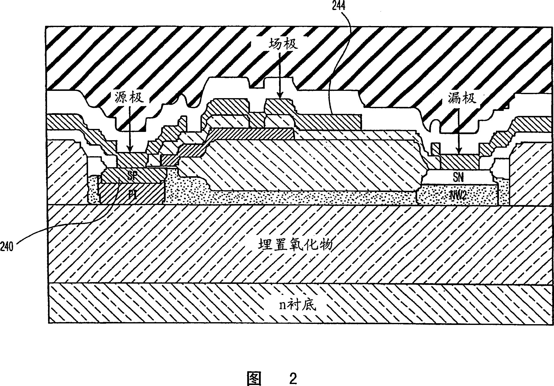
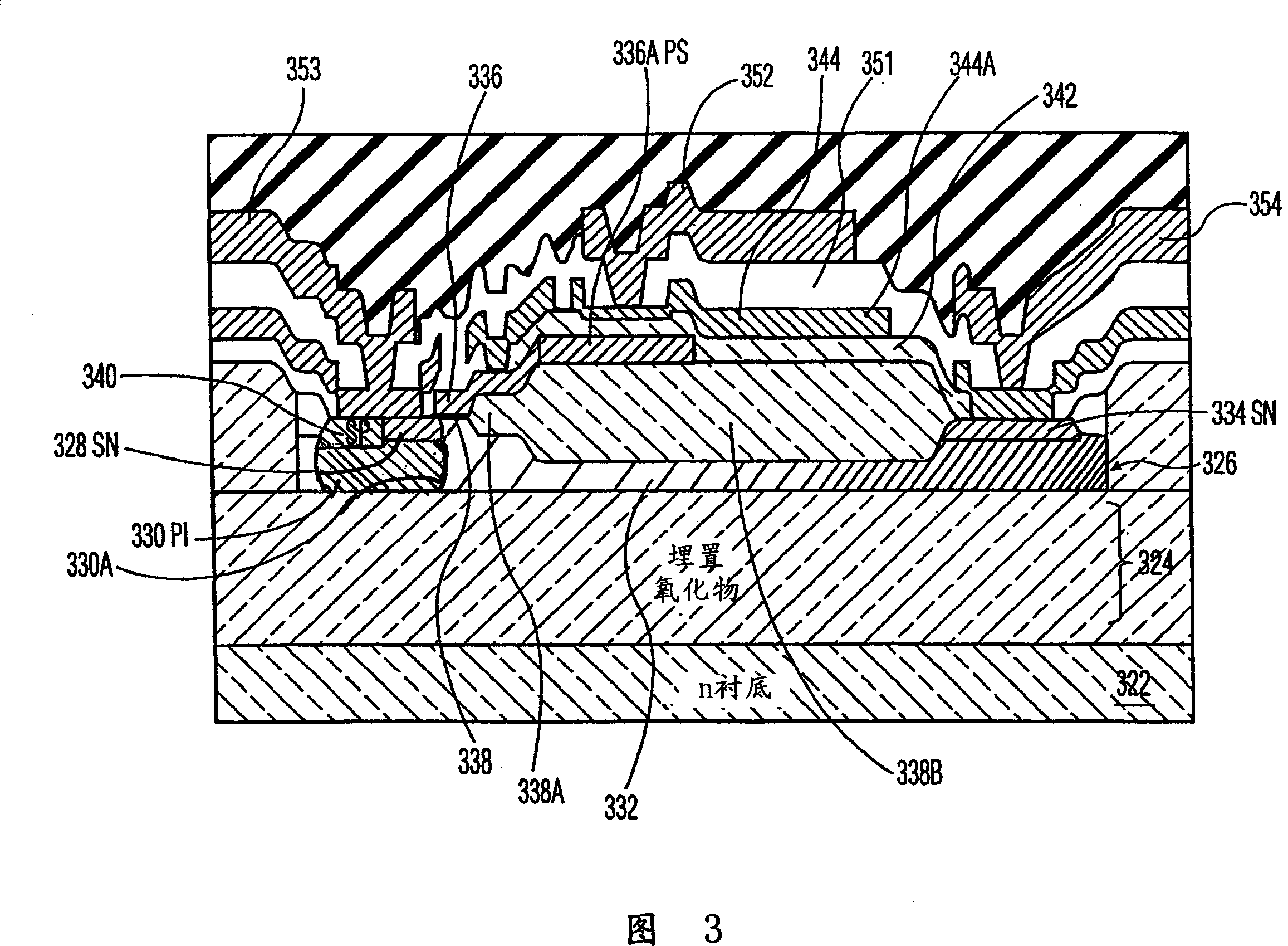
[0018] The motivation for the present invention comes from a simple idea. If a power transistor can be severely damaged by bipolar secondary breakdown, it is necessary to avoid such breakdown and to suppress and control any overvoltage breakdown. Since an avalanche in a diode does not cause bipolar secondary breakdown, we incorporate a diode structure into a transistor device and fabricate it to have a lower breakdown voltage than a transistor. Therefore, any breakdown is limited to the diode device, making the entire transistor more robust and reliable. Think of the diode region as a shock absorber or a lighting rod for transient current or voltage spikes, allowing avalanche breakdown to occur there. They absorb excess voltage and protect transistors from damage. It is easy to change the transistor structure into a diode structure by simply removing the source region of the transistor structure. Therefore, to make the integrated device, only a simple modification of the tr...


PUM


Abstract

A hybrid semiconductor device is presented in which one or more diode regions are integrated into a transistor region. In a preferred embodiment the transistor region is a continuous (self-terminating) SOI LDMOS device in which are integrated one or more diode portions. Within the diode portions, since there is only one PN junction, the mechanism for breakdown failure due to bipolar turn-on is nonexistent. The diode regions are formed such that they have a lower breakdown voltage than the transistor region, and thus any transient voltage (or current) induced breakdown is necessarily contained in the diode regions. In a preferred embodiment, the breakdown voltage of the diode portions is lowered by narrowing their field plate length relative to the transistor portion of the device. This allows the device to survive any such breakdown without being destroyed, resulting in a more rugged and more reliable device.

Description

technical field [0001] The present invention relates to the field of semiconductor devices, and more particularly, to silicon-on-insulator lateral drift metal oxide semiconductor (SOI LDMOS) devices suitable for high voltage applications. Background technique [0002] This invention is generally related to, and shares in common features with, U.S. Patent Application Serial No. 09 / 794.562, which was filed by the same applicant on February 27, 2001 (the "562" application), and is fully is hereby incorporated by reference. The '562 application provides an extensive discussion of the examples of SOI LDMOS devices discussed herein. [0003] In existing Metal Oxide Field Effect Transistor (MOSFET) devices, a conduction path is established between two regions of the same conductivity type (ie source and drain) through a region of opposite conductivity type. Current flows through this body region and the lateral drift region, while in the channel region or flow in LDMOS devices. ...

Claims


Application Information

Patent Timeline
IPC IPC(8): H01L27/02H01L27/12H01L29/06H01L27/04H01L21/762H01L21/822H01L21/8234H01L27/06H01L27/08H01L27/088H01L29/40H01L29/78H01L29/786H01L29/861
CPCH01L29/7824H01L21/76281H01L29/402H01L27/1203H01L21/76264H01L27/12
Inventor J·佩特鲁泽罗T·J·莱塔维克M·R·辛普森
Owner NXP BV
Why Eureka
Try Eureka