Reproducing method for forming die and method for making optical element
A technology for forming molds and manufacturing methods, applied in optical components, household appliances, manufacturing tools, etc., can solve problems such as unusable molds, and achieve the effect of not spending time and cost
- Summary
- Abstract
- Description
- Claims
- Application Information
AI Technical Summary
Problems solved by technology
Method used
Image
Examples
Embodiment 1
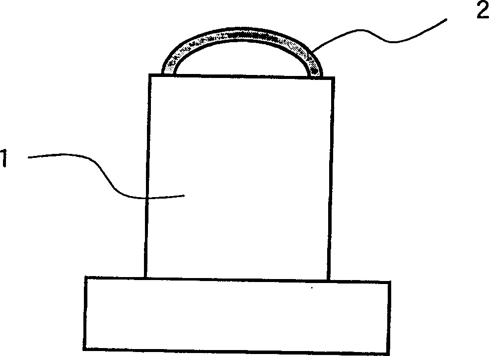
[0059] figure 1 An embodiment of an example of the mold for molding an optical element of the present invention is illustrated. figure 1 Among them, 1 is the mold base material, and 2 is a carbon-based film (release film) provided on the forming surface for forming the glass material.
[0060] First, a mold for molding an optical element will be described in detail. As the mold base material, a polycrystalline SiC formed surface produced by CVD was mirror-polished to Rmax=18 nm (roughness measurement was performed by AFM). After the mold was well cleaned, a DLC:H film was formed on the forming surface using an ion plating film forming device. As a result of analysis in the depth direction by ESCA, the thickness of the surface DLC:H film was 80 nm. As a result of microscopic Raman analysis, it was confirmed that the middle distance order (Japanese: middle distance order) between the disordered (Disordered) atomic group and the graphite (Graphite) atomic group was generated a...
Embodiment 2~6
[0073] According to Tables 1 and 2, in addition to changing the mold base material, carbon series film, release film film forming method, film thickness of the release film, optical glass, pressing conditions, cleaning before plasma treatment, and gas for etching treatment, the rest In the same manner as in Example 1, the regeneration process was repeated 100 times. According to the table, on the molding surface of the molding die, the substantial surface deterioration and the reduction in the film-forming force of the carbonaceous release film are very slight, and it is not considered that there is a problem in the appearance quality of the molded product.
Embodiment 2
[0075] Embodiment 2: outer diameter is 10mmΦ, and central wall thickness is 0.5mm, and the concave lens that コバ thick is 1.5mm;
PUM
| Property | Measurement | Unit |
|---|---|---|
| thickness | aaaaa | aaaaa |
| thickness | aaaaa | aaaaa |
| thickness | aaaaa | aaaaa |
Abstract
Description
Claims
Application Information
 - R&D Engineer
- R&D Manager
- IP Professional
- Industry Leading Data Capabilities
- Powerful AI technology
- Patent DNA Extraction
Browse by: Latest US Patents, China's latest patents, Technical Efficacy Thesaurus, Application Domain, Technology Topic, Popular Technical Reports.
© 2024 PatSnap. All rights reserved.Legal|Privacy policy|Modern Slavery Act Transparency Statement|Sitemap|About US| Contact US: help@patsnap.com


