Wafer electroplating device and method

An electroplating device and wafer technology, applied in the direction of circuits, electrolytic components, electrical components, etc., can solve problems such as escape, and achieve the effects of easy control of the gap, prevention of gas leakage, and simple design

Inactive Publication Date: 2006-08-30
IND TECH RES INST
View PDF2 Cites 6 Cited by
  • Summary
  • Abstract
  • Description
  • Claims
  • Application Information

AI Technical Summary

Problems solved by technology

[0014] The object of the present invention is to improve the existing vertical jet flow wafer electroplating method, and provide a wafer electroplating device that can adjust the tilt angle of the wafer arbitrarily, so that the gas generated by electroplating can easily escape from the electroplating surface of the wafer

Method used


Image

  • Wafer electroplating device and method
  • Wafer electroplating device and method
  • Wafer electroplating device and method

Examples


Embodiment Construction

[0073] The following are only specific examples, and are described in detail with diagrams, so as to have a further understanding and understanding of the various functions and characteristics of this creation:

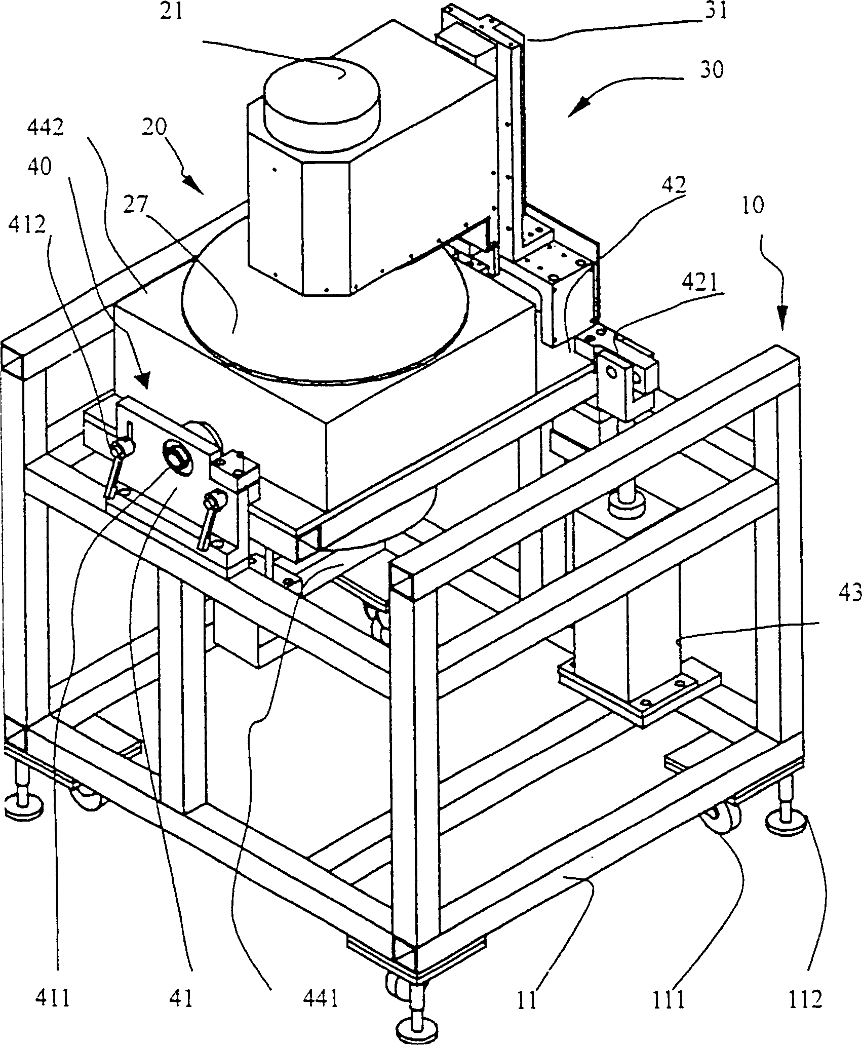
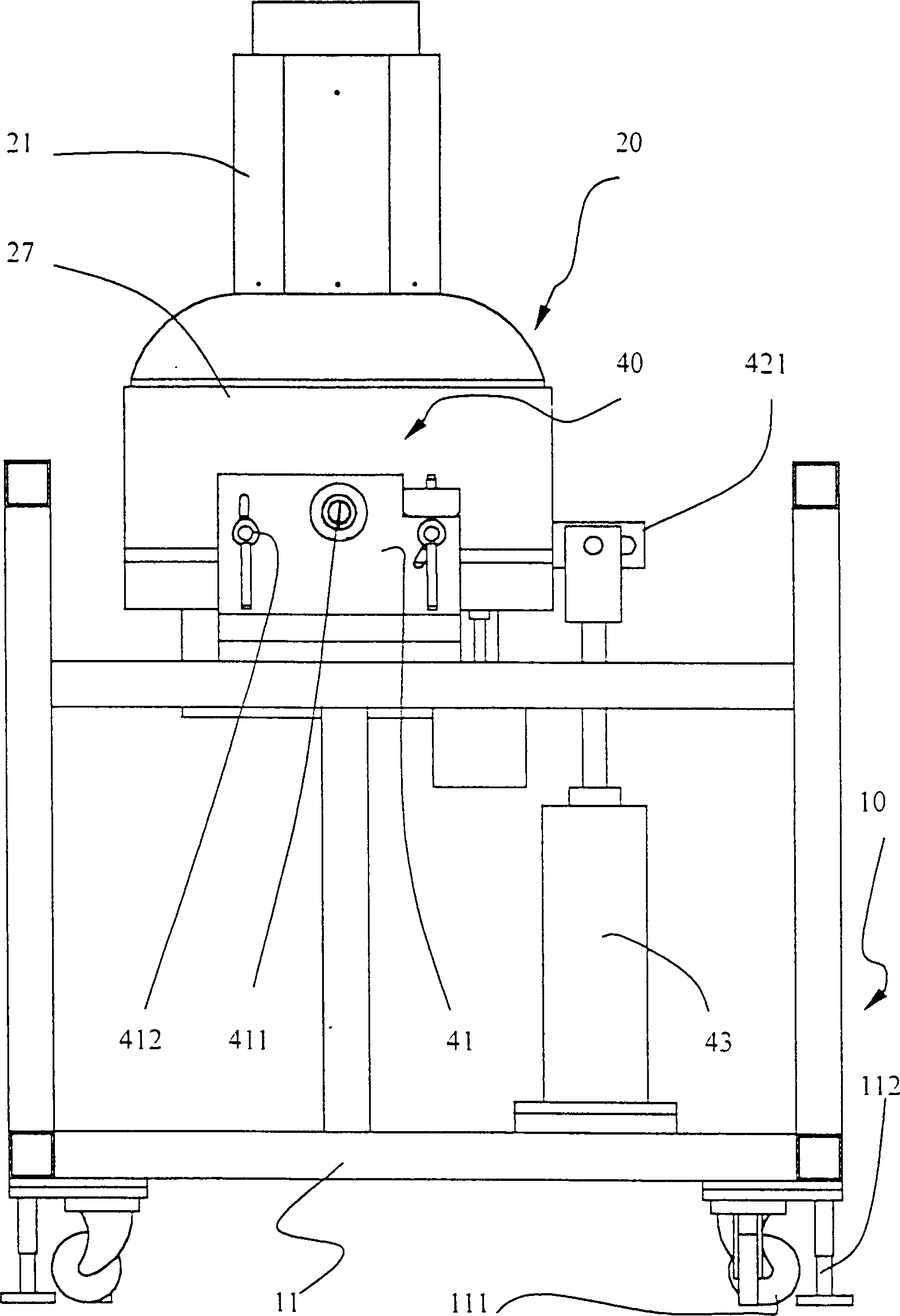
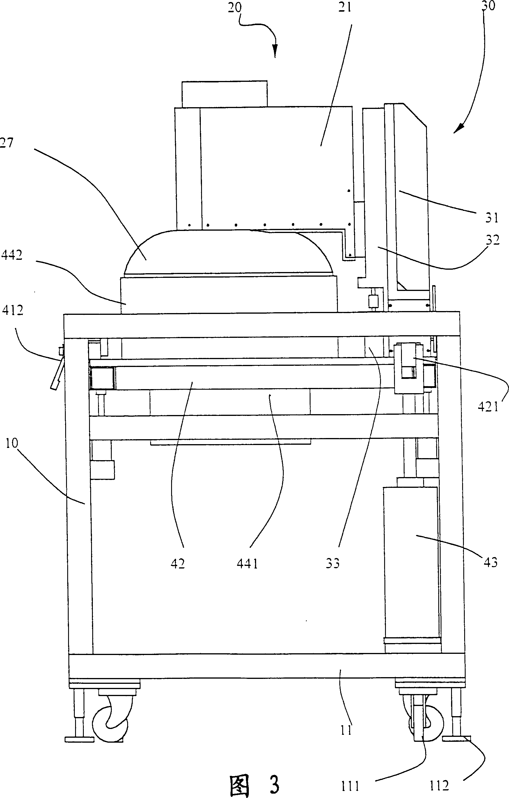
[0074] Such as Figure 1~4 Shown, the electroplating device structure of the present invention comprises:

[0075] The frame main body module 10 is provided with a frame body 11 that can be placed stably for the assembly of the main constituent modules. Nearly four corners of the frame body 11 are provided with wheel bodies 111 and adjustable support The column 112 enables the frame body 11 to be slidable and fixed, and the frame body 11 is also provided with related pipeline units and control units;

[0076] The wafer rotation module 20 is provided with a housing 21 for one side to be connected with the vertical upper and lower modules 30, and a wafer rotation mechanism is set in the housing 21, and the wafer rotation mechanism is composed of a pneumatic rotary join...


PUM


Abstract

The present invention relates to a wafer electroplating equipment and its method, belonging to vertical fountain type. Its equipment structure includes wafer rotating module, vertical upward-downward module, wafer inclining module and machine frame main body module, and the wafer rotating module containing wafer holder and rotating shaft and wafer inclining module containing plating bath unit are placed on a rotary table, a coupling device (for example cylinder) is used for driving them and making them wafer and plating bath unit simultaneously produce proper inclination. Said invention also provides its electroplating method and concrete steps, and can obtain good wafer electroplated quality.

Description

technical field [0001] The invention relates to a wafer surface electrochemical processing method, in particular to a wafer electroplating device and method. technical background [0002] In the wafer electroplating method using vertical jet flow, a uniform plating thickness can be obtained by rotating the wafer for electroplating. The biggest difference between this electroplating method and the bath type (Bath Type) is that the fixture is not fully immersed in the plating solution Dry contact in (Dry Contact). [0003] The vertical jet flow method is to place the wafer above the plating tank. The bubbles generated during the electroplating reaction process are easy to adhere to the electroplating surface of the wafer, causing the electroplating reaction to terminate at the place where the bubbles are present, and then to cause electroplating defects. In order to avoid the above-mentioned If there are defects, the wafer will be tilted at an angle so that the air bubbles ca...

Claims


Application Information

Patent Timeline
Patent Type & Authority Patents(China)
IPC IPC(8): C25D7/12C25D5/08C25D17/06H01L21/288H01L21/445H01L21/68
Inventor 杜陈忠蒋邦民王致诚黄振荣
Owner IND TECH RES INST
Why Eureka
Try Eureka