Glass passivating method for preparing RF mesa Si diode
A silicon diode and glass passivation technology, applied in semiconductor/solid-state device manufacturing, electrical components, circuits, etc., can solve problems such as complexity, low work efficiency, and difficulty in forming conformal films, and achieve high efficiency, convenient operation, and consistency good sex effect
- Summary
- Abstract
- Description
- Claims
- Application Information
AI Technical Summary
Problems solved by technology
Method used
Image
Examples
Embodiment 1
[0024] Example 1: PIN Switching Diode
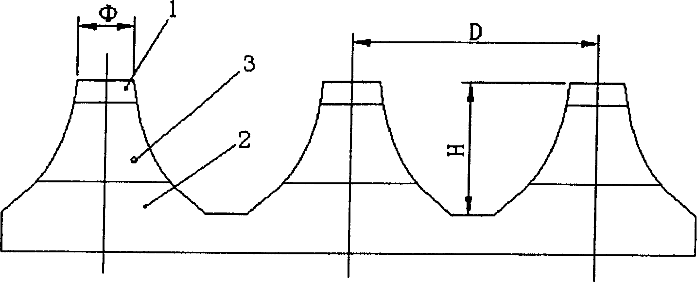
[0025] Chip size Mesa diameter Φ 135μm~150μm
[0026] Mesa height H 35μm~40μm
[0027] Adjacent die spacing D 330μm
[0028] P + N - Junction depth 1.0μm~2.0μm
[0029] N - Layer thickness 15μm~20μm
[0030] N + N - Junction depth 100μm~120μm
[0031] Process steps:
[0032] 1. Strict chemical cleaning and drying of the corroded wafers.
[0033] 2. Use a dropper to evenly coat the prepared glass slurry on the surface of the silicon wafer.
[0034] 3. Use a scraper to scrape off the glass slurry along the top of the table.
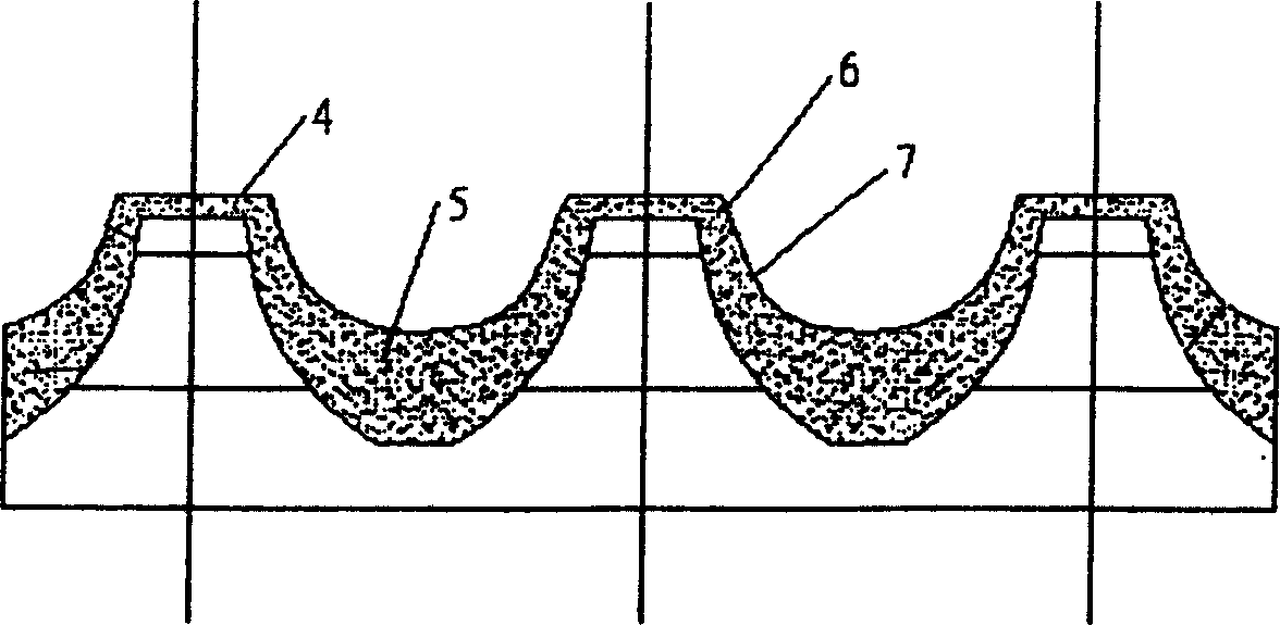
[0035] 4. Dry under infrared lamps to form a pre-deposited glass powder layer that undulates along the table.
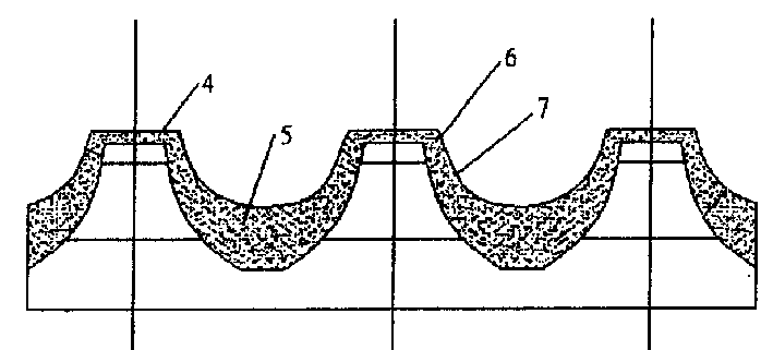
[0036] 5. Send the silicon wafer into the high-temperature furnace, degas it in the degassing temperature zone of 550°C-580°C for 10 minutes, then enter the softening zone of the glass at 700°C-800°C, and preform for 10 minutes to form ...
Embodiment 2
[0039] Example 2: PIN Attenuation Diode
[0040] Chip size Mesa diameter Φ 85μm~95μm
[0041] Mesa height H 40μm~50μm
[0042] Adjacent die spacing D 330μm
[0043] P + N - Junction depth 2.8μm~3.2μm
[0044] N - Layer thickness 15μm~20μm
[0045] N + N - Junction depth 100μm~120μm
[0046] Process steps:
[0047] 1. Strict chemical cleaning and drying of the corroded wafers.
[0048] 2. Use a dropper to evenly coat the prepared glass slurry on the surface of the silicon wafer.
[0049] 3. Use a scraper to scrape off the glass slurry along the top of the table.
[0050] 4. Dry under infrared lamps to form a pre-deposited glass powder layer that undulates along the table.
[0051] 5. Send the silicon wafer into the high-temperature furnace, degas it in the degassing temperature zone of 550°C-580°C for 10 minutes, then enter the softening zone of the glass at 700°C-800°C, and preform for 15 minutes to form ...
PUM
| Property | Measurement | Unit |
|---|---|---|
| thickness | aaaaa | aaaaa |
Abstract
Description
Claims
Application Information
 - R&D
- Intellectual Property
- Life Sciences
- Materials
- Tech Scout
- Unparalleled Data Quality
- Higher Quality Content
- 60% Fewer Hallucinations
Browse by: Latest US Patents, China's latest patents, Technical Efficacy Thesaurus, Application Domain, Technology Topic, Popular Technical Reports.
© 2025 PatSnap. All rights reserved.Legal|Privacy policy|Modern Slavery Act Transparency Statement|Sitemap|About US| Contact US: help@patsnap.com


