Forming device and method for precisely forming high-frequency and high-speed printed circuit board

A printed circuit board, precision molding technology, applied in the direction of printed circuit, printed circuit manufacturing, electrical components, etc., can solve the problems of reducing product molding quality, reducing product accuracy, low molding accuracy, etc., to improve product molding quality, improve Forming precision, compact structure

Active Publication Date: 2022-08-09
SICHUAN HAIYING ELECTRONICS TECH
View PDF11 Cites 3 Cited by
  • Summary
  • Abstract
  • Description
  • Claims
  • Application Information

AI Technical Summary

Problems solved by technology

[0005] I. Workers only apply high-frequency materials to the top surface of high-speed printed circuit boards based on experience, and then scrape off excess high-frequency materials with a scraper. It is difficult to ensure that the position of the high-frequency layer in each product is consistent with the high-speed printed circuit board. The position of the printed circuit board is consistent, which greatly reduces the accuracy of the formed product and cannot meet the needs of customers.
[0006] II. The high-speed printed circuit board is fixed on the worktable through the pressure plate in the clamping mechanism of the pressure plate, and the bottom surface of the finished high-frequency high-speed printed circuit board is firmly attached to the table. When the finished product is taken away, the edge of the product is often caused Bending deformation, which undoubtedly further reduces the molding quality of the product, and there is a technical defect of low molding accuracy

Method used


Image

  • Forming device and method for precisely forming high-frequency and high-speed printed circuit board
  • Forming device and method for precisely forming high-frequency and high-speed printed circuit board
  • Forming device and method for precisely forming high-frequency and high-speed printed circuit board

Examples


Embodiment Construction

[0038] The present invention will be further described below in conjunction with the accompanying drawings, and the protection scope of the present invention is not limited to the following:

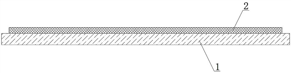
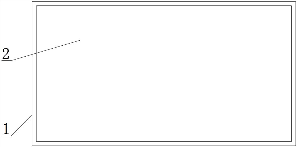
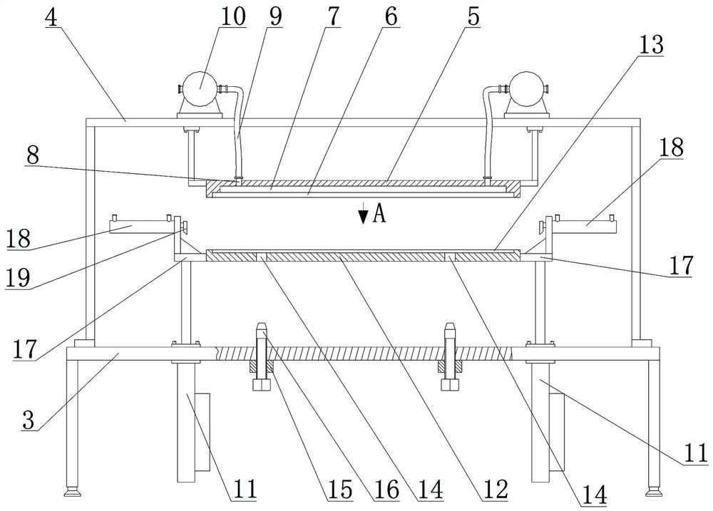
[0039] like Figure 3~4 As shown, a molding device for precision molding of high-frequency and high-speed printed circuit boards includes a gantry 4 fixed on the top surface of the workbench 3, and a cover plate 5 is fixed on the bottom surface of the beam of the gantry 4. The bottom surface of the plate 5 is provided with a groove 6, the bottom of the groove 6 is provided with a sinker 7, the cover plate 5 is provided with a joint 8 that communicates with the sinker 7, and the joint 8 is connected with a hose 9 , the other end of the hose 9 is connected with a pump 10; the inner wall of the sink 7 is coated with Teflon material to avoid high-frequency materials from sticking to the inner wall of the sink; the inner wall of the joint 8 is coated with It is covered with Teflon material t...


PUM


Abstract

The invention discloses a forming device and method for precisely forming a high-frequency and high-speed printed circuit board, a jacking electric cylinder (11) is fixedly arranged on the table top of a workbench (3), a piston rod of the jacking electric cylinder (11) penetrates through the workbench (3), a positioning plate (12) is fixedly arranged at the extending end of the jacking electric cylinder (11), and a positioning groove (13) located under a groove (6) is formed in the top surface of the positioning plate (12); two through holes (14) penetrating through the bottom surface of the positioning plate (12) are formed in the groove bottom of the positioning groove (13), two jacking mechanisms arranged under the through holes (14) respectively are arranged on the table top of the workbench (3), each jacking mechanism comprises a nut (15) welded to the bottom surface of the workbench (3), and an ejector rod (16) is in threaded connection with the interior of each nut (15). The high-frequency high-speed printed circuit board forming device has the advantages of being compact in structure, improving the forming precision of finished high-frequency high-speed printed circuit boards, improving the forming quality of products and being easy to operate.

Description

technical field [0001] The invention relates to the technical field of the production of high-frequency and high-speed printed circuit boards in electronic components, in particular to a molding device and method for precision molding of high-frequency and high-speed printed circuit boards. Background technique [0002] Electronic components include PCB boards, multilayer circuit boards, high-speed printed circuit boards, high-frequency printed boards, etc. The types of electronic components used in different electronic devices are different. Among them, high-speed printed circuit boards are mainly used in large-scale mechanical equipment. In order to improve the signal transmission frequency of high-speed printed circuit boards, the process requires the top surface of high-speed printed circuit boards. A high-frequency layer is formed to obtain the high-frequency printed circuit board required by customers, wherein the high-frequency layer can improve the electrical perform...

Claims


Application Information

Patent Timeline
IPC IPC(8): H05K3/00
CPCH05K3/00H05K2203/171H05K2203/15H05K2203/0139Y02P10/25
Inventor 陶应辉李旭李俊
Owner SICHUAN HAIYING ELECTRONICS TECH
Why Eureka
Try Eureka