Preparation method of solar cell and solar cell
A technology of solar cells and amorphous silicon layers, which is applied in the direction of circuits, electrical components, semiconductor devices, etc., can solve problems such as difficulty in achieving large-scale industrial mass production, slow development of back contact cells, and complicated manufacturing processes, and achieve self-alignment The effect of quasi-etching insulation, realizing selective removal, and simplifying the preparation process steps
- Summary
- Abstract
- Description
- Claims
- Application Information
AI Technical Summary
Problems solved by technology
Method used
Image
Examples
preparation example Construction
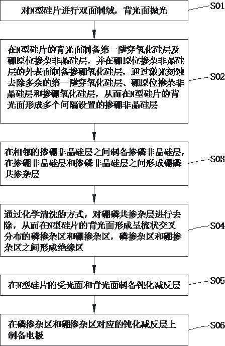
[0034] Please also refer to figure 1 , the preparation method of a solar cell provided by the present invention will now be described. The method for preparing a solar cell comprises the following steps:
[0035] S01: Double-sided texturing of N-type silicon wafers, and backlit surface polishing;
[0036] S02: prepare a first tunneling silicon oxide layer and a boron in-situ doped amorphous silicon layer on the backlight surface of the N-type silicon wafer, and prepare a boron-doped silicon oxide layer on the outer surface of the boron in-situ doped amorphous silicon layer, The redundant first tunneling silicon oxide layer, the boron in-situ doped amorphous silicon layer and the boron-doped silicon oxide layer are removed by laser etching, so as to form a plurality of boron-doped amorphous silicon oxide layers arranged at intervals on the backlight surface of the N-type silicon wafer silicon layer;
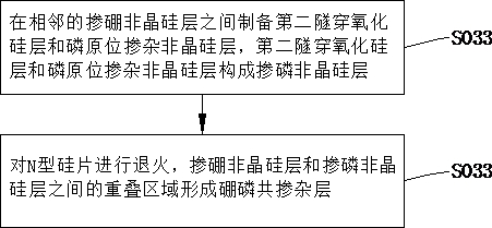
[0037] S03: prepare a phosphorus-doped amorphous silicon layer between adj...
Embodiment 1
[0059] S01: Double-sided texturing of N-type silicon wafers, and backlit surface polishing.
[0060] S02: prepare a first tunneling silicon oxide layer and a boron in-situ doped amorphous silicon layer on the backlight surface of the N-type silicon wafer, and prepare a boron-doped silicon oxide layer on the outer surface of the boron in-situ doped amorphous silicon layer, The thickness of the first tunneling silicon oxide layer is 1.5 nm, the thickness of the boron in-situ doped amorphous silicon layer is 120 nm, and the doping concentration of the boron in-situ doped amorphous silicon layer is 3E19 atm / cm 3 , the thickness of the boron-doped silicon oxide layer is 100nm, and the doping concentration of the boron-doped silicon oxide layer is 3E19 atm / cm 3 .
[0061] The redundant first tunneling silicon oxide layer, the boron in-situ doped amorphous silicon layer and the boron-doped silicon oxide layer are removed by laser etching, so as to form a plurality of boron-doped amo...
Embodiment 2
[0078] S01: Double-sided texturing of N-type silicon wafers, and backlit surface polishing.
[0079] S02: prepare a first tunneling silicon oxide layer and a boron in-situ doped amorphous silicon layer on the backlight surface of the N-type silicon wafer, and prepare a boron-doped silicon oxide layer on the outer surface of the boron in-situ doped amorphous silicon layer, The thickness of the first tunneling silicon oxide layer is 1.5 nm, the thickness of the boron in-situ doped amorphous silicon layer is 120 nm, and the doping concentration of the boron in-situ doped amorphous silicon layer is 3E19 atm / cm 3 , the thickness of the boron-doped silicon oxide layer is 100nm, and the doping concentration of the boron-doped silicon oxide layer is 3E19 atm / cm 3 ;
[0080] The redundant first tunneling silicon oxide layer, the boron in-situ doped amorphous silicon layer and the boron-doped silicon oxide layer are removed by laser etching, so as to form a plurality of boron-doped amo...
PUM
| Property | Measurement | Unit |
|---|---|---|
| thickness | aaaaa | aaaaa |
| width | aaaaa | aaaaa |
| width | aaaaa | aaaaa |
Abstract
Description
Claims
Application Information
 - R&D
- Intellectual Property
- Life Sciences
- Materials
- Tech Scout
- Unparalleled Data Quality
- Higher Quality Content
- 60% Fewer Hallucinations
Browse by: Latest US Patents, China's latest patents, Technical Efficacy Thesaurus, Application Domain, Technology Topic, Popular Technical Reports.
© 2025 PatSnap. All rights reserved.Legal|Privacy policy|Modern Slavery Act Transparency Statement|Sitemap|About US| Contact US: help@patsnap.com


