Display device
A technology for a display device and a display area, which is applied to identification devices, antenna supports/mounting devices, antennas, etc., can solve problems such as weakening and affecting NFC performance, and achieve high magnetic field strength and guarantee NFC performance.
- Summary
- Abstract
- Description
- Claims
- Application Information
AI Technical Summary
Problems solved by technology
Method used
Image

Examples
example 1
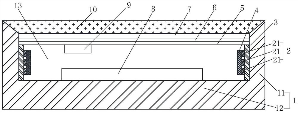
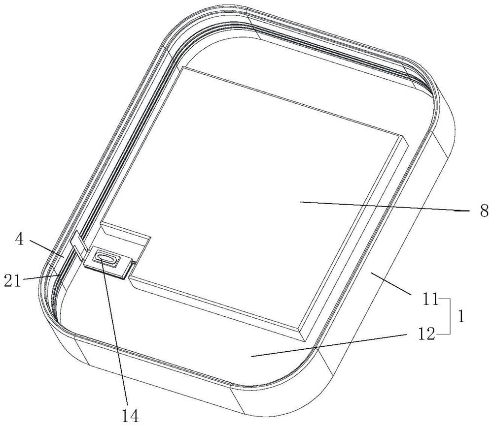
[0047] like figure 1 , figure 2 As shown, the display device includes a casing 1 and a display panel 7; the casing 1 includes a bottom wall 12 and a side wall 11 arranged around the edge of the bottom wall 12, the bottom wall 12 and the side wall 11 An installation cavity 13 having an opening is enclosed, and the display panel 7 is disposed in the opening; the installation cavity 13 can install components such as the lithium battery 8 and the NFC IC 14 . The fan-out area 70 of the display panel 7 is connected with the flexible circuit board 50, the front of the display panel 7 covers the cover plate 10, the cover plate 10 can be a glass cover plate, and the back of the display panel 7 is bonded with SCF (Super Cleaner) through the adhesive layer 6. Foam; ultra clean foam) layer 5, the material of the adhesive layer 6 can be but not limited to BF glue (nitrile butadiene rubber), the side of the SCF layer 5 away from the adhesive layer is provided with an IC (Integrated Circui...
example 2
[0051] like image 3 , Figure 4 As shown, the main difference between Example 2 and Example 1 is that the NFC antenna 2 is provided in the display panel 7 .
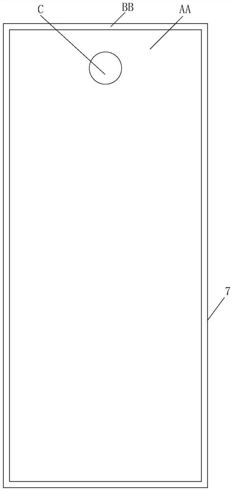
[0052] Specifically, the display panel 7 includes a display area AA and a non-display area BB surrounding the display area AA; the display area AA has an under-screen camera light-transmitting area C; wherein, the under-screen camera light-transmitting area C and its surrounding areas The stacked structure includes a substrate 31 , a first PI layer 32 , a barrier layer 33 , a second PI layer 34 , a first planarization layer 35 , a first metal wiring layer 42 , a second planarization layer 36 , and a passivation layer 37 arranged in sequence , a first transparent wiring layer, a third planarization layer 38 , a second transparent wiring layer and a fourth planarization layer 39 . The first transparent wiring layer and the second transparent wiring layer serve as the first conductive layers 41 and 42, respectively.
[...
example 3
[0057] like Figure 5 , Image 6 As shown, the main difference between Example 3 and Example 1 is that the NFC antenna 2 is provided in the display panel 7.
[0058] Specifically, the display panel 7 includes a display area AA and a non-display area BB surrounding the display area AA; the wires 21 of the NFC antenna 2 are arranged along the edge of the display area AA.
[0059] The stacked structure of the display panel 7 includes a substrate 31 , a first PI layer 32 , a barrier layer 33 , a first metal wiring layer, a second PI layer 34 , a first planarization layer 35 , and a second metal wiring layer 47 , which are arranged in sequence. , a passivation layer 37 , a second planarization layer 36 , a third metal wiring layer 46 , an optical adhesive layer 43 , a touch electrode layer 45 and an encapsulation layer 44 .
[0060] The first metal wiring layer serves as one of the first conductive layers 42 . The first metal wiring layer includes a conductive pattern 421 and th...
PUM
 Abstract
Description
Claims
Application Information
 - R&D
- Intellectual Property
- Life Sciences
- Materials
- Tech Scout
- Unparalleled Data Quality
- Higher Quality Content
- 60% Fewer Hallucinations
Browse by: Latest US Patents, China's latest patents, Technical Efficacy Thesaurus, Application Domain, Technology Topic, Popular Technical Reports.
© 2025 PatSnap. All rights reserved.Legal|Privacy policy|Modern Slavery Act Transparency Statement|Sitemap|About US| Contact US: help@patsnap.com