Impedance configuration device of memory interface

A memory interface and configuration device technology, applied in static memory, digital memory information, information storage, etc., can solve the problems of pin line reflection, signal transmission and other problems

Pending Publication Date: 2022-07-22
SILICON MOTION INC (CN)
View PDF0 Cites 0 Cited by
  • Summary
  • Abstract
  • Description
  • Claims
  • Application Information

AI Technical Summary

Problems solved by technology

[0003] After the speed of the DRAM (Dynamic Random Access Memory DRAM) bus reaches a high transfer rate, such as 500Mb / s or higher, system-level signaling problems may occur, for example, from connected peer devices (such as controllers, DRAM modules, etc.)

Method used

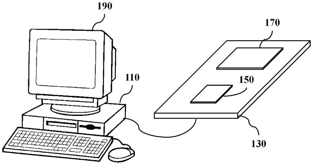
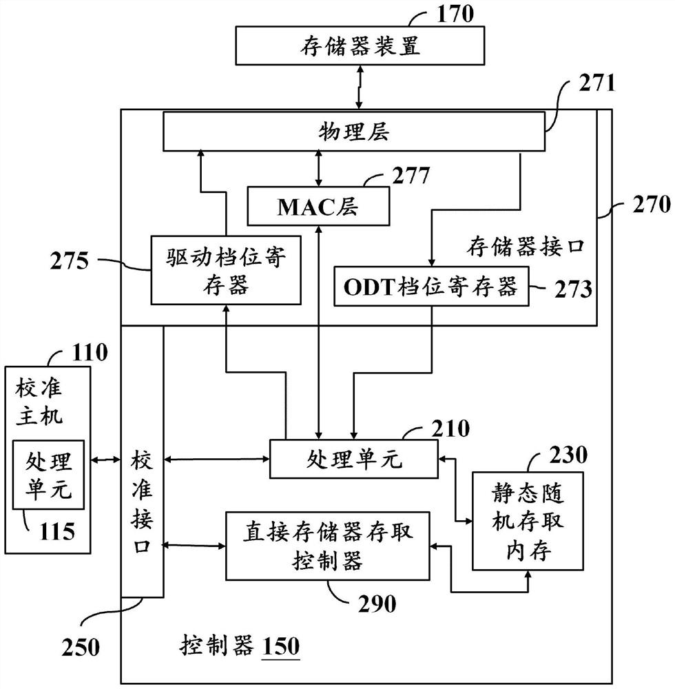
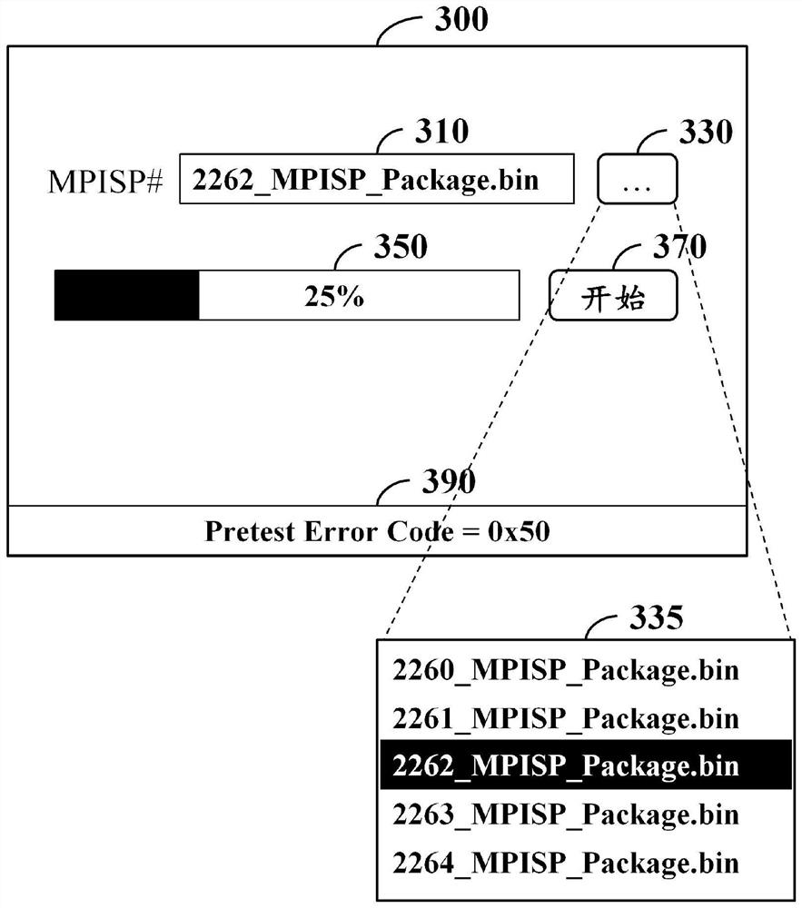

Image

  • Impedance configuration device of memory interface
  • Impedance configuration device of memory interface
  • Impedance configuration device of memory interface

Examples


Embodiment Construction

[0046] The embodiments of the present invention will be described below with reference to the related drawings. In the figures, the same reference numbers refer to the same or similar components or method flows.

[0047] It must be understood that words such as "comprising" and "including" used in this specification are used to indicate the existence of specific technical features, values, method steps, job processes, components and / or components, but do not exclude the possibility of Plus more technical features, values, method steps, job processes, components, components, or any combination of the above.

[0048] The use of words such as "first", "second" and "third" in the present invention is used to modify the components in the claims, and is not used to indicate that there is a priority order, a precedence relationship, or a component precedence Another component, or the chronological order in which method steps are executed, is only used to distinguish components with ...


PUM


Abstract

An impedance configuration device for a memory interface includes a processing unit coupled to a memory interface, a non-volatile memory, and a calibration interface. The processing unit sets a first resistance value of an in-chip terminating resistor associated with the first receiver as a first default resistance value; setting a second resistance value of a driving variable resistor associated with a second transmitter as a second default resistance value; performing a test for a plurality of test combinations, each combination including a third resistance value associated with the driving variable resistor of the first transmitter and a fourth resistance value associated with the on-chip termination resistor of the second receiver; and storing the test result of each test combination to a specific position of the non-volatile memory, so that the calibration host can obtain the test result of each test combination from the non-volatile memory.

Description

[0001] This application is a divisional application, the application date of the original application is: March 20, 2019; the application number is: 201910211851.3; the name of the invention is: impedance configuration method for memory interface and computer-readable storage medium. technical field [0002] The present invention relates to a communication interface, in particular to an impedance configuration device for a memory interface. Background technique [0003] After the speed of the Dynamic Random Access Memory (DRAM) bus reaches a high transfer rate, such as 500Mb / s or higher, system-level signaling problems may occur, for example, from connected peer devices (such as controllers, DRAM modules, etc.) pin lines produce reflections. The above-mentioned signal transmission problem can be solved by adjusting the driver (Driver) and the on-die termination resistor (On-Die Termination ODT). Therefore, the present invention provides a configuration device for a memory i...

Claims


Application Information

Patent Timeline
Patent Type & Authority Applications(China)
IPC IPC(8): G11C29/50G11C29/56
CPCG11C29/50008G11C29/56G11C2207/2254G11C29/028G11C29/022G06F3/0632G11C7/1048G11C29/38G06F3/0614G06F3/0673
Inventor 宋威良张启彬
Owner SILICON MOTION INC (CN)
Why Eureka
Try Eureka