
Chemical mechanical polishing pad and preparation method thereof

A chemical-mechanical and polishing pad technology, applied in the field of polishing pads, can solve the problems of decreased elasticity of the polishing cloth, not satisfying the polishing pad at the same time, and damage to the followability.

Pending Publication Date: 2022-07-05
宁波赢伟泰科新材料有限公司 +1
View PDF0 Cites 1 Cited by
  • Summary
  • Abstract
  • Description
  • Claims
  • Application Information

AI Technical Summary

Problems solved by technology

If an attempt is made to thicken the foam portion of the small finger-shaped cells to prolong the life of the polishing pad, it will result in a thinner support layer for the sponge-shaped cells, a decrease in the size of the sponge cells, and a decrease in the elasticity of the polishing cloth, thereby compromising followability, affecting semiconductors The flatness of the silicon wafer; if you try to increase the thickness of the support layer to improve the followability and cushioning, the small finger-shaped foam part will become thinner and the service life will decrease
That is, in the preparation of polishing pads by the traditional one-stage condensation film-forming method, one of the buffer function and product life is sacrificed, and there is no polishing pad that satisfies both functions at the same time.

Method used


Image

  • Chemical mechanical polishing pad and preparation method thereof
  • Chemical mechanical polishing pad and preparation method thereof
  • Chemical mechanical polishing pad and preparation method thereof

Examples


preparation example Construction

[0036] The invention provides a preparation method of a chemical mechanical polishing pad, and the preparation method comprises the following steps:

[0037] Step 1: stirring and mixing the materials, vacuuming and defoaming after mixing to prepare resin slurry;

[0038] Step 2: The film-forming substrate is coated with a release agent, and the resin slurry is blade-coated on the film-forming substrate

[0039] Step 3: The film-forming substrate is coagulated for the first time, and the coagulation time is 0.5-5 minutes to obtain a peelable semi-cured resin slurry, and the semi-cured resin slurry is removed from the film-forming substrate. peel off;

[0040] Step 4: performing a second coagulation on the semi-cured resin slurry peeled from the film-forming substrate, the coagulation time is more than 10 minutes, and a polishing pad is obtained after processing;

[0041] The vacuum deaeration is completed by a vacuum deaeration mixer, which is a stirring and mixing equipment ...

Embodiment 1

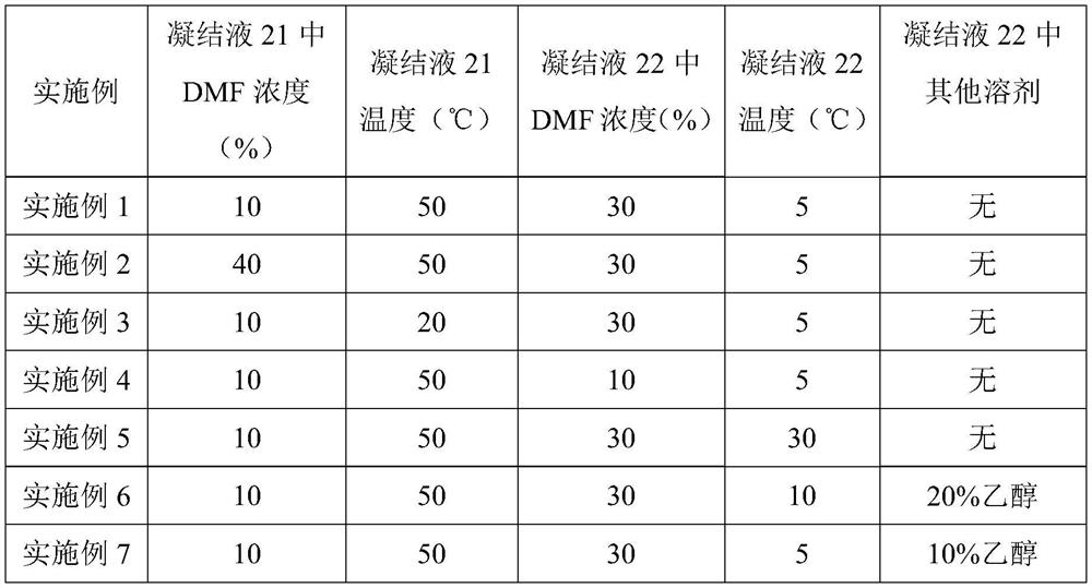
[0071] Example 1: as figure 2 As shown, a preparation method of a two-stage condensed film-forming polishing pad is provided, and the preparation method comprises:

[0072] Step 1: stirring and mixing the materials, vacuuming and defoaming after mixing to prepare resin slurry 51;

[0073] Step 2: The film-forming substrate 41 is coated with a release agent, and the resin slurry is blade-coated on the film-forming substrate

[0074] Step 3: The film-forming substrate enters the coagulation liquid 21, and the first coagulation is performed. The coagulation time is 1.5 minutes to obtain a peelable semi-cured resin slurry, and the semi-cured resin slurry is removed from the The film substrate is peeled off, and the peeling occurs in the coagulation liquid 22;

[0075] Step 4: The resin slurry in the semi-cured state peeled off on the film-forming substrate is coagulated for the second time in the coagulation liquid 22, and the coagulation time is 15 minutes, and a polishing pad...

Embodiment 2

[0076] Example 2: as figure 2 As shown, a preparation method of a two-stage condensed film-forming polishing pad is provided, and the preparation method comprises:

[0077] Step 1: stirring and mixing the materials, vacuuming and defoaming after mixing to prepare resin slurry 51;

[0078] Step 2: The film-forming substrate 41 is coated with a release agent, and the resin slurry is blade-coated on the film-forming substrate

[0079]Step 3: The film-forming substrate enters the coagulation liquid 21, and the first coagulation is performed. The coagulation time is 1.5 minutes to obtain a peelable semi-cured resin slurry, and the semi-cured resin slurry is removed from the The film substrate is peeled off, and the peeling occurs in the coagulation liquid 22;

[0080] Step 4: The resin slurry in the semi-cured state peeled off on the film-forming substrate is coagulated for the second time in the coagulation liquid 22, and the coagulation time is 15 minutes, and a polishing pad ...


PUM


Abstract

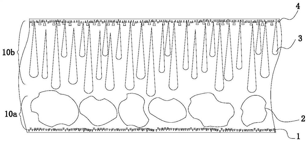
The invention relates to a chemical mechanical polishing pad and a preparation method thereof. According to the chemical mechanical polishing pad, polyurethane resin slurry is used and smeared on a film forming base material coated with a release agent, and different hole structures are coagulated on the two sides of a coagulated film in two steps in a two-section coagulation mode. In the process of condensation and pore forming, the concentration and temperature of two sections of condensation liquid are controlled, so that pores of two different pore structures are formed in the same condensation film at the same time, the diameter of finger-shaped pores which account for at least 15% of the total thickness of the condensation film from the surface layer to the inside is not larger than 25 microns, and the finger-shaped pores formed in the second layer side are high in pore diameter uniformity, small in pore diameter and large in abradable thickness; the service life of the polishing pad is prolonged; the sponge-shaped holes are formed in the side of the first layer, the thickness of the sponge-shaped holes accounts for one third or more than one third of the total thickness of the condensation film, the followability of a to-be-polished object is good, flexible support is provided, and the surface planarization degree of the to-be-polished object is improved.

Description

technical field [0001] The present invention relates to the technical field of chemical mechanical polishing used in the manufacture of semiconductor chips, and more particularly, the present invention relates to a polishing pad manufactured by a two-stage condensation film-forming process for chemical mechanical polishing (CMP) of semiconductor chips, which can prolong the service life of the polishing pad , a polishing pad that improves the flatness of the surface of the object to be polished. Background technique [0002] Chemical Mechanical Polishing (CMP) is a very important process in the production of semiconductor chips. Semiconductor chips are made by integrating multi-layer micro-circuit structures on silicon wafers. Many different materials are used in the manufacture of micro-integrated circuits. Deposition technology and process, step-by-step layer deposition on the surface of the semiconductor wafer, and then remove unnecessary parts through chemical etching, t...

Claims


Application Information

Patent Timeline
IPC IPC(8): B29C41/24B29C41/46B24B37/24B24D18/00B29K75/00B29L7/00
CPCB29C41/24B29C41/46B29C41/003B24B37/24B24D18/009B29K2075/00B29L2007/002
Inventor 相红旗陈浩聪姚力军
Owner 宁波赢伟泰科新材料有限公司
Learn More