
Dual one-dimensional micro-electro-mechanical mirror element

A micro-electro-mechanical and micro-electro-mechanical scanning technology, applied in optical components, instruments, optics, etc., can solve the problems of poor imaging quality, expensive production costs, and adjustment of mirror size to achieve the effect of ensuring clarity

Pending Publication Date: 2022-07-01
MILLENNIUM KEYSTONE TECH CO LTD
View PDF1 Cites 0 Cited by
  • Summary
  • Abstract
  • Description
  • Claims
  • Application Information

AI Technical Summary

Problems solved by technology

However, the micro-electromechanical micro-mirror element 60 is manufactured using a semiconductor manufacturing process, which is not only expensive to manufacture, but also difficult to adjust the size of the mirror (the mask needs to be redesigned), the position of the mirror according to different projection requirements, and the light-transmitting top 64 and the light-transmitting bottom 65 can fully transmit light, and its incident light 67 is easily affected by ambient light, which makes the final image quality worse; therefore, it is necessary to improve

Method used


Image

  • Dual one-dimensional micro-electro-mechanical mirror element
  • Dual one-dimensional micro-electro-mechanical mirror element
  • Dual one-dimensional micro-electro-mechanical mirror element

Examples


Embodiment Construction

[0037] Below in conjunction with accompanying drawing, structure principle and working principle of the present invention are described in detail:

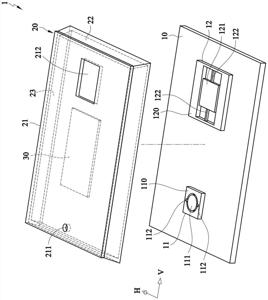
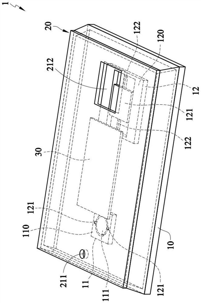
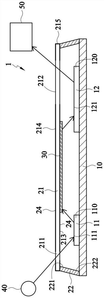
[0038] First see figure 1 As shown, it is the first embodiment of the dual one-dimensional MEMS mirror element 1 of the present invention, which includes a substrate 10, a first one-dimensional MEMS scanning chip 11, a second one-dimensional MEMS scanning chip 12, an upper A cover 20 and a reflective layer 30, wherein the first one-dimensional MEMS scanning chip 11 and the second one-dimensional MEMS scanning chip 12 are welded on the substrate 10, and the upper cover 20 is disposed on the substrate 10 to cover Combined with the first one-dimensional MEMS scanning chip 11 and the second one-dimensional MEMS scanning chip 12 , the reflective layer 30 is disposed on the inner top surface 23 of the upper cover.

[0039] The above-mentioned substrate 10 may be a ceramic substrate, but not limited thereto.

[0040] The above-mention...


PUM


Abstract

The invention provides a dual one-dimensional micro-electro-mechanical mirror element, which comprises a substrate, a first one-dimensional micro-electro-mechanical scanning chip, a second one-dimensional micro-electro-mechanical scanning chip and an upper cover, the first and second one-dimensional micro-electro-mechanical scanning chips are welded on the substrate; the upper cover is fixed on the substrate so as to cover the first and second one-dimensional micro-electro-mechanical scanning chips therein, and the upper cover forms a first window and a second window corresponding to the first and second one-dimensional micro-electro-mechanical scanning chips; the first one-dimensional micro-electro-mechanical scanning chip and the second one-dimensional micro-electro-mechanical scanning chip which are manufactured in advance are arranged at different positions on the same substrate, so that vibration interference applied to a vibration environment can be overcome easily, and the light-transmitting area of the upper cover is only the first window and the second window and can transmit light. The light incident to the first and second one-dimensional micro-electro-mechanical scanning chips can be effectively prevented from being influenced by ambient light.

Description

technical field [0001] The present invention relates to a microelectromechanical mirror element, in particular to a double one-dimensional microelectromechanical mirror element. Background technique [0002] The existing projection equipment adopts a micro-electromechanical scanning device to project the generated image beam to form a projection screen. At present, the MEMS scanning device of projection equipment mainly consists of two MEMS mirror scanning chips. Each of the MEMS mirror scanning chips includes a mirror element to project the projection screen. The mirror of one MEMS mirror scanning chip is controlled along the horizontal axis. (H-axis) rotation, while the mirror element of another MEMS mirror scanning chip is controlled to rotate along the vertical axis (V-axis). Since the mirror is a rotatable structure, when the projection equipment is used in a vibrating environment, the vibration force will shake the mirror elements of the two MEMS mirror scanning chips...

Claims


Application Information

Patent Timeline
Patent Type & Authority Applications(China)
IPC IPC(8): G02B26/08G02B26/10
CPCG02B26/0833G02B26/105
Inventor 不公告发明人
Owner MILLENNIUM KEYSTONE TECH CO LTD
Learn More