Wafer cleaning device and cleaning method

A technology for cleaning devices and wafers, applied in cleaning methods and utensils, cleaning methods using liquids, chemical instruments and methods, etc., can solve problems such as reducing and reducing wafer yield, and achieve the effect of improving consistency

Pending Publication Date: 2022-06-24
INST OF MICROELECTRONICS CHINESE ACAD OF SCI +1
View PDF4 Cites 0 Cited by
  • Summary
  • Abstract
  • Description
  • Claims
  • Application Information

AI Technical Summary

Problems solved by technology

[0003] However, in the process of cleaning multiple wafers at the same time, since the liquid inlet of the liquid infusion pipe is opened at one end of the liquid infusion pipe, and is limited by the pressure used to transmit the cleaning liquid, the nozzles far away from the liquid inlet will not affect the corresponding wafer. The cleaning effect is significantly different from the effect of the nozzles near the liquid inlet on the corresponding wafer cleaning, that is, the effect of the nozzle on the wafer cleaning decreases as the distance between the nozzle and the liquid inlet increases, thereby reducing the wafer Yield

Method used


Image

  • Wafer cleaning device and cleaning method

Examples


Embodiment 1

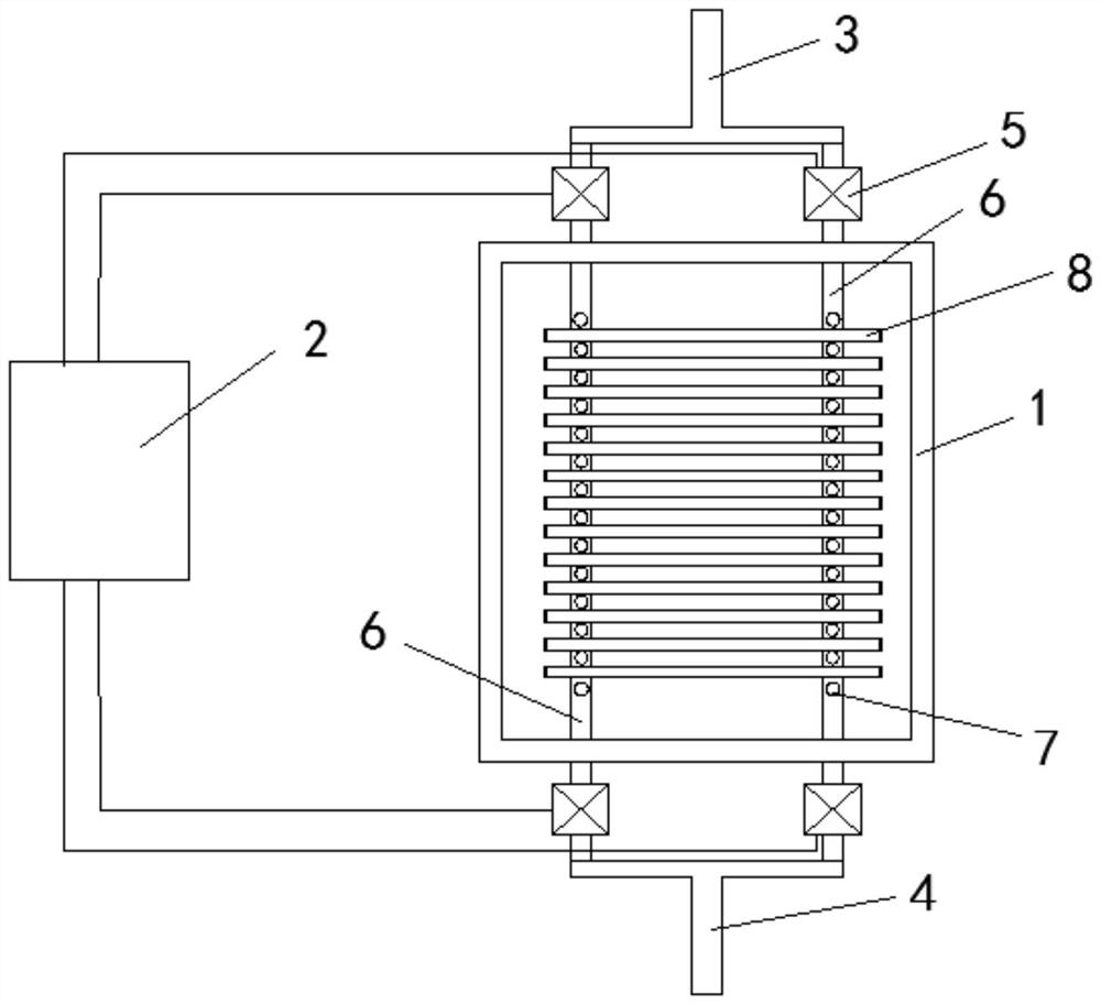
[0034] This embodiment provides a wafer cleaning device, which combines figure 1 , the wafer cleaning device includes: a cleaning tank 1 , an electronic control module 2 , a first infusion manifold 3 , a second infusion manifold 4 , four solenoid valves 5 and two infusion tubes 6 . Wherein, the two infusion tubes 6 are parallel to each other, and the two ends of each infusion tube 6 respectively penetrate the bottom of the two opposite side walls of the cleaning tank 1; the two ends of each infusion tube 6 are respectively provided with a liquid inlet; Each infusion pipe 6 is fixedly provided with a plurality of nozzles 7 along the length direction, and the nozzles 7 are all located in the cleaning tank 1; the first infusion main pipe 3 and the second infusion main pipe 4 are respectively located on opposite sides of the cleaning tank 1, and the two The liquid inlets of each infusion pipe 6 are respectively communicated with the corresponding first infusion main pipe 3 or the ...

Embodiment 2

[0039] The present embodiment provides a wafer cleaning method, including: providing two infusion pipes 6 , a plurality of nozzles 7 are arranged in the longitudinal direction of the two infusion pipes 6 , and the plurality of nozzles 7 are used for spraying the cleaning liquid on the wafer 8 , Both ends of the two infusion pipes 6 are respectively provided with a liquid inlet; the cleaning liquid is conveyed to the infusion pipes 6 through the liquid inlets, so that the nozzles 7 can clean the wafers 8 in the cleaning tank 1 .

[0040] Further, the method also includes: providing four solenoid valves 5, and the four solenoid valves 5 are respectively fixedly arranged at both ends of each infusion pipe 6; the flow rate of the cleaning liquid conveyed by the infusion pipe 6 is controlled by the solenoid valve 5, so that it is easy to change. The cleaning degree of the cleaning solution to the wafer 8 .

[0041] Further, the method further includes: providing an electronic contr...


PUM


Abstract

The invention provides a wafer cleaning device and a cleaning method. The wafer cleaning device comprises at least one liquid conveying pipe; the at least one liquid conveying pipe is provided with a plurality of nozzles in the length direction; the at least one infusion tube is provided with a plurality of liquid inlets, and two of the plurality of liquid inlets are respectively positioned at two ends of the infusion tube. According to the wafer cleaning device, the cleaning effect of all the nozzles on the same liquid conveying pipe on the wafers can be guaranteed, and the corrosion uniformity between different wafers in the wafer cleaning device is improved.

Description

technical field [0001] The present invention relates to the technical field of semiconductor processing, and in particular, to a wafer cleaning device and a cleaning method. Background technique [0002] With the rapid development of industrial production technology, in the process of wafer cleaning, tank cleaners are commonly used cleaning equipment. The existing tank wafer cleaning method usually uses multiple wafers arranged in parallel and spaced, and placed together for cleaning The tank is cleaned and different wafers are cleaned simultaneously through multiple nozzles. [0003] However, in the process of cleaning multiple wafers at the same time, since the liquid inlet of the infusion tube is opened at one end of the infusion tube, and is limited by the pressure used to transmit the cleaning liquid, the nozzles away from the liquid inlet are not suitable for the corresponding wafers. The cleaning effect is obviously different from the cleaning effect of the nozzle ne...

Claims


Application Information

Patent Timeline
Patent Type & Authority Applications(China)
IPC IPC(8): B08B3/02B08B3/08B08B13/00H01L21/67H01L21/673
CPCB08B3/02B08B3/08B08B13/00H01L21/67051H01L21/67309H01L21/67346
Inventor 姜喆求卢一泓李琳胡艳鹏王佳张月
Owner INST OF MICROELECTRONICS CHINESE ACAD OF SCI
Why Eureka
Try Eureka