Pixel circuit and display panel

A pixel circuit and potential technology, applied in static indicators, instruments, etc., can solve the problems of multi-thin film transistors, affecting the viewing effect, and the display effect is not obvious, so as to save signal transmission lines, improve uniformity, and increase the displayable area. Effect

Pending Publication Date: 2022-06-21
TCL CHINA STAR OPTOELECTRONICS TECH CO LTD
View PDF0 Cites 2 Cited by
  • Summary
  • Abstract
  • Description
  • Claims
  • Application Information

AI Technical Summary

Problems solved by technology

[0002] The continuous development and progress of display technology has brought increasingly rich display products, and the hybrid drive scheme of PWM (Pulse Width Modulation, Pulse Width Modulation) & PAM (Pulse Amplitude Modulation, Pulse Amplitude Modulation) has gradually appeared, but because the hybrid drive scheme requires more With many thin film transistors, detection and compensation face major challenges
[0003] However, with the scheme of PWM&PAM hybrid driving, since the turn-on voltage of each thin film transistor in the display panel is different, the display effect of PWM&PAM hybrid driving is not obvious, which affects the viewing effect

Method used


Image

  • Pixel circuit and display panel
  • Pixel circuit and display panel
  • Pixel circuit and display panel

Examples


Embodiment Construction

[0027] The technical solutions in the embodiments of the present application will be clearly and completely described below with reference to the accompanying drawings in the embodiments of the present application. Obviously, the described embodiments are only a part of the embodiments of the present application, but not all of the embodiments. Based on the embodiments in the present application, all other embodiments obtained by those skilled in the art without creative work fall within the protection scope of the present application.

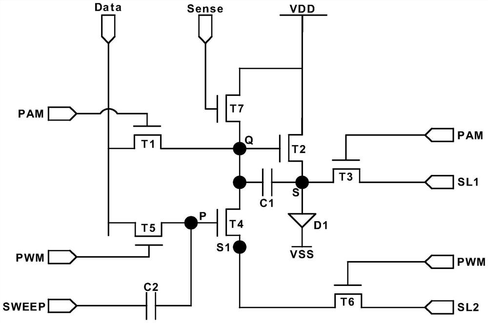
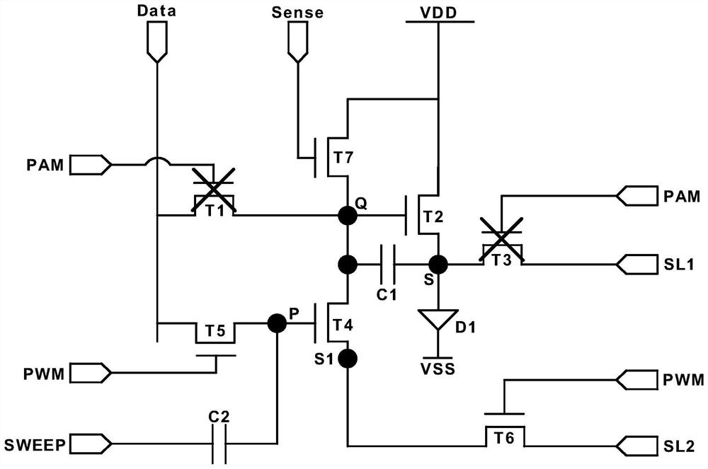
[0028] This embodiment provides a pixel circuit, please refer to Figure 1 to Figure 8 ,like figure 1 As shown, the pixel circuit includes a driving transistor T2, a first transistor T4, a second transistor T5 and a third transistor T6, the drain of the first transistor T4 is connected to the gate of the driving transistor T2; the source of the second transistor T5 / One of the drains is connected to the gate of the first transistor T4, the ...


PUM


Abstract

The invention discloses a pixel circuit and a display panel, and the pixel circuit comprises a driving transistor, a first transistor, a second transistor, and a third transistor. By connecting one of the source electrode/drain electrode of the third transistor with the source electrode of the first transistor, connecting the other one of the source electrode/drain electrode of the third transistor with the first sensing line, and connecting the grid electrode of the third transistor with the pulse width control end, the source electrode potential of the first transistor can be obtained through the first sensing line and the third transistor; therefore, the first transistor is realized, and the uniformity of picture display is improved.

Description

technical field [0001] The present application relates to the field of display technology, and in particular, to a pixel circuit and a display panel. Background technique [0002] The continuous development and progress of display technology bring more and more display products, and the hybrid drive scheme of PWM (Pulse Width Modulation) & PAM (Pulse Amplitude Modulation) has gradually emerged, but due to the need for more hybrid drive schemes. With many thin-film transistors, detection and compensation face significant challenges. [0003] However, with the PWM&PAM hybrid driving scheme, the display effect of the PWM&PAM hybrid driving is not obvious due to the different turn-on voltages of each thin film transistor in the display panel, which affects the viewing effect. [0004] Therefore, it is necessary to propose a detection scheme for PWM&PAM hybrid drive to perform external compensation to achieve the uniformity of picture display. SUMMARY OF THE INVENTION [0005...

Claims


Application Information

Patent Timeline
Patent Type & Authority Applications(China)
IPC IPC(8): G09G3/30G09G3/32G09G3/3225
CPCG09G3/30G09G3/32G09G3/3225G09G2320/0233
Inventor 刘桉语王利民
Owner TCL CHINA STAR OPTOELECTRONICS TECH CO LTD
Why Eureka
Try Eureka