Electromagnetic shielding film and circuit board

An electromagnetic shielding film and circuit board technology, applied in the field of electronics, can solve the problems of unsatisfactory roughness of the insulating layer, poor bonding strength between the insulating layer and the shielding layer, delamination between the insulating layer and the shielding layer, etc. the effect of strength

Pending Publication Date: 2022-06-17
GUANGZHOU FANGBANG ELECTRONICS
View PDF0 Cites 0 Cited by
  • Summary
  • Abstract
  • Description
  • Claims
  • Application Information

AI Technical Summary

Problems solved by technology

[0005] The inventor found in the process of implementing the present invention that there are the following technical problems in the prior art: in the process of pressing the existing electromagnetic shielding film to the circuit board, the glue of the adhesive film layer is easily separated from the electromagnetic shielding film and the circuit board. The edge between the boards overflows, whi

Method used


Image

  • Electromagnetic shielding film and circuit board
  • Electromagnetic shielding film and circuit board
  • Electromagnetic shielding film and circuit board

Examples


Example Embodiment

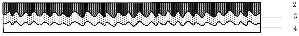
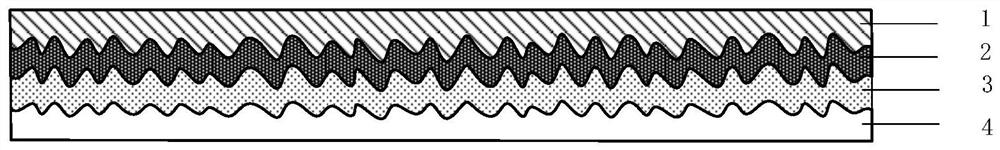
[0065]具体地,当所述电磁屏蔽膜包括载体层1、绝缘层2、屏蔽层3、胶膜层4及保护膜层5时,所述电磁屏蔽膜的制备方法包括:

[0066]1)准备载体层1;

[0067]2)在载体层1的一面上形成绝缘层2;

[0068]3)在绝缘层2的远离载体层1的一面上形成屏蔽层3;

[0069]4)在屏蔽层3的远离绝缘层2的一面上涂覆胶而形成胶膜层4;

[0070]5)在胶膜层4的远离屏蔽层3的一面上贴合保护膜层5。

Example Embodiment

[0072]实施例一:

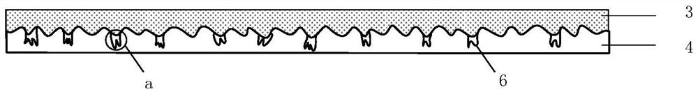
[0073]一种电磁屏蔽膜,包括绝缘层、屏蔽层及胶膜层;所述屏蔽层形成于所述绝缘层的一面上,所述胶膜层设于所述屏蔽层的远离所述绝缘层的一面上;其中,所述绝缘层的靠近所述屏蔽层的一面的粗糙度Rz为0.09微米,所述胶膜层的胶克重参数为0.01克每平方分米,所述绝缘层的靠近所述屏蔽层的一面的粗糙度Rz与所述胶膜层的胶克重参数两者的数值的比例为9。

[0074]测试结果:经过测试,本实施例的电磁屏蔽膜的所述绝缘层和所述屏蔽层之间的分离拉力大于12.23N / cm,本实施例的电磁屏蔽膜压合到线路板后胶膜层的胶溢出的长度小于78μm。

[0075]由此可见,通过应用本实施例的所述电磁屏蔽膜,能够提高电磁屏蔽膜的绝缘层与屏蔽层之间的接着强度,避免在弯折电磁屏蔽膜时容易使得绝缘层与屏蔽层之间出现分层的现象,并且在将所述电磁屏蔽膜压合到线路板后,所述电磁屏蔽膜与线路板之间具有良好的粘合强度的同时,还能让线路板具有良好的外观。

Example Embodiment

[0076]实施例二:

[0077]一种电磁屏蔽膜,包括绝缘层、屏蔽层及胶膜层;所述屏蔽层形成于所述绝缘层的一面上,所述胶膜层设于所述屏蔽层的远离所述绝缘层的一面上;其中,所述绝缘层的靠近所述屏蔽层的一面的粗糙度Rz为14.68微米,所述胶膜层的胶克重参数为1克每平方分米,所述绝缘层的靠近所述屏蔽层的一面的粗糙度Rz与所述胶膜层的胶克重参数两者的数值的比例为14.68。

[0078]测试结果:经过测试,本实施例的电磁屏蔽膜的所述绝缘层和所述屏蔽层之间的分离拉力大于16.78N / cm,本实施例的电磁屏蔽膜压合到线路板后胶膜层的胶溢出的长度小于90μm。

[0079]由此可见,通过应用本实施例的所述电磁屏蔽膜,能够提高电磁屏蔽膜的绝缘层与屏蔽层之间的接着强度,避免在弯折电磁屏蔽膜时容易使得绝缘层与屏蔽层之间出现分层的现象,并且在将所述电磁屏蔽膜压合到线路板后,还能让线路板具有良好的外观。


PUM

PropertyMeasurementUnit
Roughnessaaaaaaaaaa
Roughnessaaaaaaaaaa
Roughnessaaaaaaaaaa

Abstract

The invention relates to the technical field of electronics, and discloses an electromagnetic shielding film and a circuit board wherein the electromagnetic shielding film comprises an insulating layer, a shielding layer and an adhesive film layer; the shielding layer is formed on one surface of the insulating layer, and the adhesive film layer is arranged on one surface, far away from the insulating layer, of the shielding layer; wherein under the condition that the unit of the roughness Rz is micron and the unit of the adhesive gram weight parameter is gram per square decimeter, the ratio of the roughness Rz of one surface, close to the shielding layer, of the insulating layer to the value of the adhesive gram weight parameter of the adhesive film layer is 5-200. The electromagnetic shielding film and the circuit board provided by the invention can simultaneously have the following advantages: the phenomenon of layering between the insulating layer and the shielding layer is not easy to occur, and the circuit board has good appearance after being pressed on the circuit board.

Description

technical field [0001] The invention relates to the field of electronic technology, in particular to an electromagnetic shielding film and a circuit board. Background technique [0002] With the rapid development of the electronics industry, electronic products are further developed toward miniaturization, light weight, and high-density assembly, which greatly promotes the development of flexible circuit boards, thereby realizing the integration of component devices and wire connections. Flexible circuit boards can be widely used in industries such as mobile phones, liquid crystal displays, communications and aerospace. [0003] Driven by the international market, functional flexible circuit boards dominate the flexible circuit board market, and an important indicator for evaluating the performance of functional flexible circuit boards is Electromagnetic Interference Shielding (EMI Shielding). With the integration of functions of communication equipment such as mobile phone...

Claims


Application Information

Patent Timeline
IPC IPC(8): H05K1/02H05K9/00
CPCH05K9/0081H05K1/02
Inventor 苏陟张美娟
Owner GUANGZHOU FANGBANG ELECTRONICS
Why Eureka
Try Eureka