
LED backlight module preparation method and LED backlight module

A technology of backlight modules and LED chips, which is applied to identification devices, instruments, semiconductor devices, etc., and can solve the problems of large overall thickness and high cost of LED backlight modules

Pending Publication Date: 2022-05-31
HUIZHOU JUFEI OPTOELECTRONICS CO LTD
View PDF0 Cites 0 Cited by
  • Summary
  • Abstract
  • Description
  • Claims
  • Application Information

AI Technical Summary

Problems solved by technology

[0005] In view of the deficiencies of the above-mentioned related technologies, the purpose of this application is to provide a method for preparing an LED backlight module and an LED backlight module, aiming at solving the problem of large overall thickness and high cost of the LED backlight module

Method used


Image

  • LED backlight module preparation method and LED backlight module
  • LED backlight module preparation method and LED backlight module
  • LED backlight module preparation method and LED backlight module

Examples


preparation example Construction

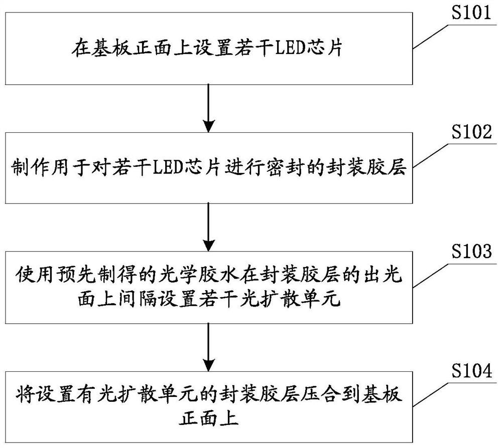
[0044] The embodiment of the present invention provides a method for preparing an LED backlight module, see figure 1 As shown, it includes the steps:

[0045] S101: setting several LED chips on the front surface of the substrate.

[0046] In this step, each LED chip is fixed on the front surface of the substrate, and each LED chip is evenly distributed on the front surface of the substrate according to a preset array layout.

[0047] S102: Making an encapsulation adhesive layer for sealing a plurality of LED chips.

[0048]The encapsulation adhesive layer is used for sealing and protecting the LED chips arranged on the front surface of the substrate.

[0049] S103: Using pre-made optical glue, arranging several light diffusion units at intervals on the light-emitting surface of the encapsulation glue layer.

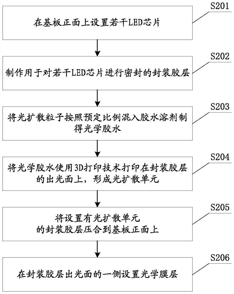
[0050] Before this step, it also includes mixing the light diffusion particles into the glue solvent according to a predetermined ratio to prepare optical glue. This s...


PUM


Abstract

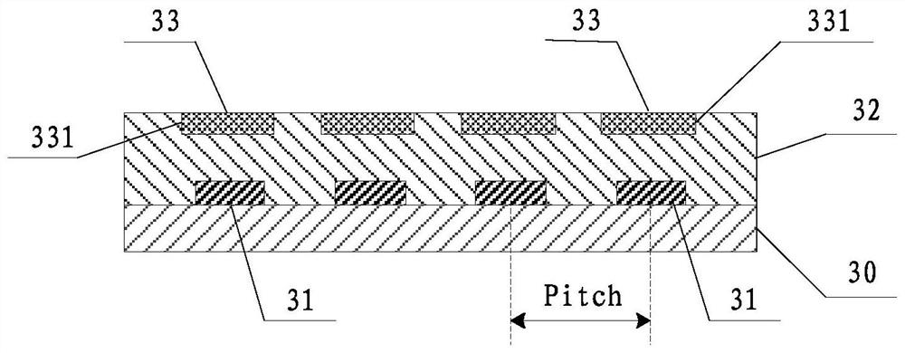
The LED backlight module preparation method comprises the steps that a plurality of LED chips are arranged on the front face of a substrate, a packaging glue layer used for sealing the LED chips is manufactured, a plurality of light diffusion units are arranged on the light emitting face of the packaging glue layer at intervals through optical glue prepared in advance, and the light diffusion units are arranged on the light emitting face of the packaging glue layer at intervals. The light diffusion unit is used for reflecting and refracting light rays emitted by the LED chips, so that the light rays emitted by the LED chips can be uniformly emitted from the light emitting surface of the packaging adhesive layer; the packaging adhesive layer provided with the light diffusion units is pressed on the front face of the substrate, the LED chips are wrapped by the packaging adhesive layer, and the light diffusion units are pressed into the packaging adhesive layer and located above the LED chips; according to the backlight module manufactured through the method, the light diffusion unit above the LED chip in the packaging adhesive layer enables light emitted by the LED chip to be evenly emitted out of the light emitting face of the packaging adhesive layer, a light uniformizing diaphragm is omitted, the overall thickness of the backlight module is reduced, and cost is reduced.

Description

technical field [0001] The invention relates to the field of display technology, in particular to a method for preparing an LED backlight module and an LED backlight module. Background technique [0002] LED display can integrate information release, entertainment, and publicity functions, and as an emerging high-tech product, with its rich technological content, majestic appearance, smooth display screen, and delicate color performance, it can be an environmental protection Add a new vitality and set up a moving landscape. [0003] With the continuous development of Mini LED products, smart end users' demands for thinner products such as tablets, laptops, and monitors are gradually emerging. The display module of the LED display screen is composed of multiple pixel units, so it is necessary to convert the point light source emitted by each pixel unit into a surface light source. In related technologies, the conversion of point light sources into surface light sources is a...

Claims


Application Information

Patent Timeline
IPC IPC(8): H01L25/075H01L33/54H01L33/58H01L33/60G09F9/33
CPCH01L25/0753H01L33/54H01L33/58H01L33/60G09F9/33H01L2933/005H01L2933/0058
Inventor 郑斌
Owner HUIZHOU JUFEI OPTOELECTRONICS CO LTD
Learn More