
Subminiature double-port output GaN fast charging device

An ultra-small, PCB board technology, applied in the direction of output power conversion devices, circuit devices, transportation and packaging, etc., can solve the problem of low power density, etc., to reduce volume, reduce impact, and effectively use space structure effect

Pending Publication Date: 2022-05-13
HUNAN JUSHEN ELECTRONICS CO LTD
View PDF8 Cites 0 Cited by
  • Summary
  • Abstract
  • Description
  • Claims
  • Application Information

AI Technical Summary

Problems solved by technology

[0002] With the development of consumer electronic products, multi-port output small-volume chargers are the future trend. At present, common power adapters and chargers have only one circuit board, and all devices are placed on one circuit board. Such a layout requires a large number of There is also a part of the power adapter. The charger will use two circuit boards, one high-voltage circuit and one low-voltage circuit. This can make full use of some space and reduce some volume, but the power density of this solution is still not enough. Very large, but also has certain limitations

Method used


Image

  • Subminiature double-port output GaN fast charging device
  • Subminiature double-port output GaN fast charging device
  • Subminiature double-port output GaN fast charging device

Examples


Embodiment Construction

[0021] The preferred embodiments of the present invention will be described below in conjunction with the accompanying drawings. It should be understood that the preferred embodiments described here are only used to illustrate and explain the present invention, and are not intended to limit the present invention.

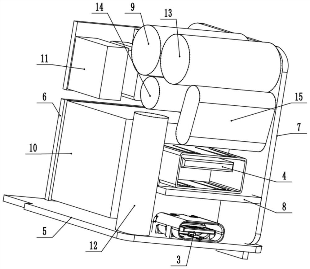
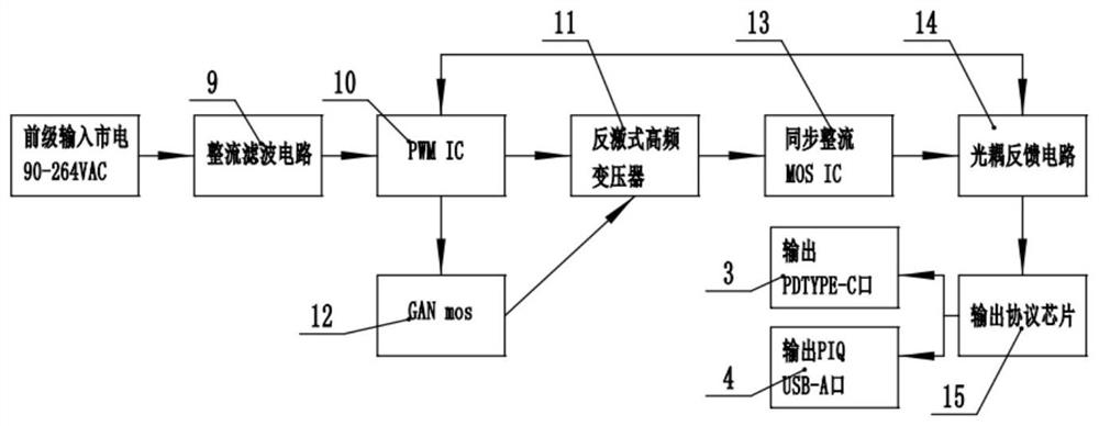
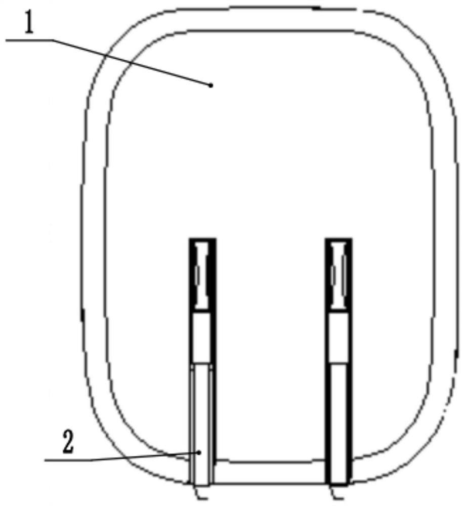
[0022] Please refer to the attached Figure 1-5 , an ultra-small dual-port output GaN fast charging device provided by the present invention includes a casing 1, and the front end of the casing 1 is rotatably connected to a pin 2, so the pin 2 can have a folding function, which effectively improves the inconvenience of carrying a charger for business trips in daily life , the rear end of the shell 1 is provided with an output PDTYPE-C port 3 and an output PIQUSB-A port 4, the first PCB board 5 is fixedly connected to the bottom of the shell 1, the second PCB board 6 is fixedly connected to the front side of the shell 1, and the shell 1 The third PCB board 7 is fixed...


PUM


Abstract

The invention relates to the technical field of chargers, in particular to a subminiature double-port output GaN fast charging device which comprises a shell, an output PDTYPE-C port and an output PIQUSB-A port are formed in the rear end of the shell, a first PCB is fixedly connected to the lower portion of the interior of the shell, a second PCB is fixedly connected to the front side of the interior of the shell, and a third PCB is fixedly connected to the front side of the interior of the shell. The left side of the interior of the shell is fixedly connected with a third PCB, the lower portion of the right side wall of the third PCB is fixedly connected with a fourth PCB, the upper surface of the first PCB is fixedly connected with GAN mos, the output PDTYPE-C port is fixedly connected to the rear end of the upper surface of the first PCB, and the lower portion of the rear surface of the second PCB is fixedly connected with a PWM IC. The invention has the beneficial effects that the space structure can be effectively utilized, the volume of the charger is reduced, the heating of a power device is reduced, the power density of the charger is greatly improved, access equipment can be intelligently identified, current output can be intelligently adjusted, intelligent voltage drop compensation can be carried out and the like, and high-speed charging is realized.

Description

technical field [0001] The invention relates to the technical field of chargers, in particular to an ultra-small dual-port output GaN fast charging device. Background technique [0002] With the development of consumer electronic products, multi-port output small-volume chargers are the future trend. At present, common power adapters and chargers have only one circuit board, and all devices are placed on one circuit board. Such a layout requires a large number of There is also a part of the power adapter. The charger will use two circuit boards, one high-voltage circuit and one low-voltage circuit. This can make full use of some space and reduce some volume, but the power density of this solution is still not enough. It is large and has certain limitations. [0003] Therefore, it is necessary to invent an ultra-small dual-port output GaN fast charging device. Contents of the invention [0004] For this reason, the present invention provides an ultra-small dual-port outpu...

Claims


Application Information

Patent Timeline
Patent Type & Authority Applications(China)
IPC IPC(8): H05K7/02H05K5/02H02J7/00H02M1/00
CPCH05K7/02H05K5/026H02J7/0042H02M1/00
Inventor 詹海峰赵智星谢峰胡宪权欧炜昌冷昭君万威戴先台
Owner HUNAN JUSHEN ELECTRONICS CO LTD
Learn More