
Diffusion method for silicon wafer and photovoltaic silicon wafer

A diffusion method and silicon wafer technology, applied in diffusion/doping, chemical instruments and methods, crystal growth, etc., can solve the problem that the attenuation rate of battery efficiency needs to be reduced, the light conversion efficiency of the battery needs to be improved, and it is difficult to further improve the inside of the silicon wafer Doping concentration and other issues

Pending Publication Date: 2022-05-13
TONGWEI SOLAR (ANHUI) CO LTD
View PDF0 Cites 0 Cited by
  • Summary
  • Abstract
  • Description
  • Claims
  • Application Information

AI Technical Summary

Problems solved by technology

[0003] The current diffusion method cannot reduce the surface doping concentration of the silicon wafer very well, and it is difficult to further increase the internal doping concentration of the silicon wafer. The light conversion efficiency of the cell still needs to be improved, and the attenuation rate of the cell efficiency still needs to be reduced.

Method used


Image

  • Diffusion method for silicon wafer and photovoltaic silicon wafer
  • Diffusion method for silicon wafer and photovoltaic silicon wafer
  • Diffusion method for silicon wafer and photovoltaic silicon wafer

Examples


Embodiment 1

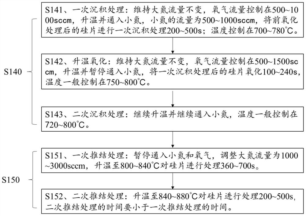
[0056] This embodiment provides a photovoltaic silicon chip, which is obtained by placing the silicon chip in a quartz boat and being treated by a diffusion method in a diffusion furnace. The specific steps of the diffusion method are as follows in order:

[0057] 1. First check whether the diffusion furnace is leaking;

[0058] 2. Send the textured silicon wafer into the diffusion furnace, and then raise the temperature to 740°C;

[0059] 3. Pre-oxidation: maintain the pressure in the furnace at 100 mbar, and treat with oxygen and nitrogen for 3 minutes; the oxygen flow rate is 1000 sccm, and the maximum nitrogen flow rate is 1000 sccm.

[0060] 4. Deposition treatment: a. One-time deposition treatment: heat up to 760°C, feed small nitrogen for 350s, the flow rate of small nitrogen is 750sccm, and the treatment time is 350s.

[0061] b. Oxidation by heating: suspend the introduction of small nitrogen, and raise the temperature to 780°C for 170s.

[0062] c. Secondary deposi...

Embodiment 2

[0070] This embodiment provides a photovoltaic silicon wafer, which is obtained after the silicon wafer is processed by a diffusion method. Compared with Embodiment 1, the specific steps of the diffusion method are mainly different in that:

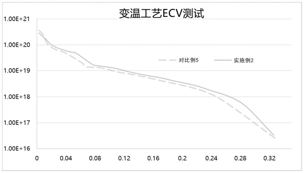
[0071] During the deposition process, the temperature of the primary deposition process is 760°C, the temperature of the secondary deposition process is 775°C, and the temperature difference between the two is 15°C.

Embodiment 3

[0073] This embodiment provides a photovoltaic silicon wafer, which is obtained after the silicon wafer is processed by a diffusion method. Compared with Embodiment 1, the specific steps of the diffusion method are mainly different in that:

[0074] During the push knot treatment, the temperature of the first knot push treatment is 830°C, and the temperature of the second push knot treatment is 840°C, and the temperature difference between the two is 10°C.


PUM


Abstract

The embodiment of the invention provides a diffusion method for a silicon wafer and a photovoltaic silicon wafer, and relates to the field of photovoltaic cells. The diffusion method for the silicon wafer comprises the following steps of: performing primary deposition treatment on the pretreated silicon wafer at the temperature of 700-780 DEG C, and then performing secondary deposition treatment at the temperature of 720-800 DEG C, the temperature of the secondary deposition treatment being higher than the temperature of the primary deposition treatment; carrying out primary junction pushing treatment on the silicon wafer at the temperature of 800-840 DEG C; carrying out secondary junction pushing treatment on the silicon wafer at the temperature of 840-880 DEG C; the temperature of the primary junction pushing treatment is higher than the temperature of the secondary deposition and lower than the temperature of the secondary junction pushing treatment. The photovoltaic silicon wafer obtained by using the diffusion method is low in surface doping concentration, high and uniform in internal doping concentration, small in surface recombination effect and long in minority carrier service life, and when the photovoltaic silicon wafer is used for a solar cell, a solar cell with high light conversion efficiency can be obtained.

Description

technical field [0001] The present application relates to the field of photovoltaic cells, in particular, to a diffusion method for silicon wafers and photovoltaic silicon wafers. Background technique [0002] In crystalline silicon solar cells, silicon wafers need to be diffused to reduce the surface doping concentration of silicon wafers and increase the internal doping concentration of silicon wafers, thereby improving the light conversion efficiency of the cell and reducing the attenuation rate of the cell. [0003] The current diffusion method cannot reduce the surface doping concentration of the silicon wafer very well, and it is also difficult to further increase the internal doping concentration of the silicon wafer. The light conversion efficiency of the cell still needs to be improved, and the attenuation rate of the cell efficiency still needs to be reduced. Contents of the invention [0004] The purpose of the embodiments of the present application is to provid...

Claims


Application Information

Patent Timeline
IPC IPC(8): H01L31/18H01L21/02C30B29/06C30B31/06
CPCH01L31/1804H01L21/02321C30B31/06C30B29/06
Inventor 李红飞徐冠群郑傲然夏伟吉克超
Owner TONGWEI SOLAR (ANHUI) CO LTD
Learn More