
Display module capable of being spliced, preparation method and display device

A display module and drive module technology, which is applied to identification devices, semiconductor/solid-state device components, instruments, etc., can solve the problems of affecting the display effect of the display screen, excessive splicing seam, large pixel pitch, etc., and achieve optimal display effect , increase the resolution, reduce the effect of pixel pitch

Pending Publication Date: 2022-05-13
FOSHAN NATIONSTAR OPTOELECTRONICS CO LTD
View PDF0 Cites 1 Cited by
  • Summary
  • Abstract
  • Description
  • Claims
  • Application Information

AI Technical Summary

Problems solved by technology

In the existing LED display screen, there is a problem that the splicing seam of the LED modules that are spliced ​​with each other is too large, so that the pixel pitch of the local area at the splicing seam is too large, which affects the overall display effect of the display screen

Method used


Image

  • Display module capable of being spliced, preparation method and display device
  • Display module capable of being spliced, preparation method and display device
  • Display module capable of being spliced, preparation method and display device

Examples


Embodiment 1

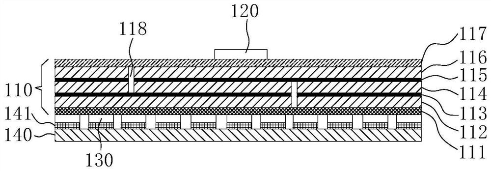
[0056] In view of the above problems, Embodiment 1 of the present invention provides a splicable display module, figure 1 A schematic structural diagram of a splicable display module provided in Embodiment 1 of the present invention, as shown in figure 1 As shown, the splicable display module includes: a circuit board 110 , a driving module 120 , a plurality of LED light-emitting chips 130 and a light-transmitting carrier substrate 140 .

[0057] Wherein, the circuit board 110 includes a first pad layer and a second pad layer oppositely arranged, and at least one circuit layer between the first pad layer and the second pad layer, the first pad layer, the second pad layer An insulating layer is arranged between two adjacent layers of the second pad layer and the at least one circuit layer. In the embodiment of the present invention, the number of circuit layers is not limited, and can be specifically set according to the complexity of the circuit, for example, the more complex...

Embodiment 2

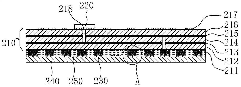
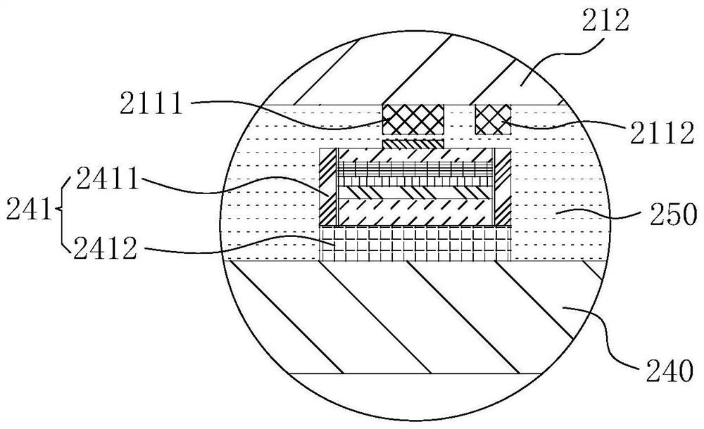
[0073] figure 2 It is a schematic structural diagram of a splicable display module provided in Embodiment 2 of the present invention, image 3 for figure 2 The enlarged view of the area A in the middle, such as figure 2 and image 3 As shown, in this embodiment, the splicable display module includes: a circuit board 210 , a driving module 220 , a plurality of LED light-emitting chips 230 and a light-transmitting carrier substrate 240 .

[0074] Wherein, the wiring board 210 includes a first pad layer 211, a first insulating layer 212, a first wiring layer 213, a second insulating layer 214, a second wiring layer 215, a third insulating layer 216 and a second pad layer stacked in sequence. Layer 217.

[0075] The LED light-emitting chip 230 is disposed on the first pad layer 211 and electrically connected to the first pad layer 211 . The driving module 220 is disposed on the second pad layer 217 and electrically connected to the second pad layer 217 . The first pad laye...

Embodiment 3

[0089] Embodiment 3 of the present invention provides a method for preparing a splicable display module, Figure 5 A schematic flow chart of a method for preparing a splicable display module provided in Embodiment 3 of the present invention, as shown in Figure 5 As shown, the method specifically includes the following steps:

[0090] S11. Providing a circuit board.

[0091] Specifically, the circuit board includes a first pad layer and a second pad layer oppositely arranged, and at least one circuit layer between the first pad layer and the second pad layer, the first pad layer, the second pad layer An insulating layer is arranged between two adjacent layers of the second pad layer and at least one circuit layer, and the first pad layer, the second pad layer and at least one circuit layer are electrically connected through conductive vias penetrating the insulating layer . Specifically, the structure of the circuit board can refer to the content described in the first embo...


PUM

PropertyMeasurementUnit
pore sizeaaaaaaaaaa
reflectanceaaaaaaaaaa

Abstract

The invention discloses a display module capable of being spliced, a preparation method and a display device.The display module comprises a light-transmitting carrier substrate, a circuit board, a driving module and a plurality of LED light-emitting wafers, the LED light-emitting wafers and the driving module are arranged on the two opposite sides of the circuit board respectively, in this way, the LED light-emitting wafers are arranged on the side, provided with the LED light-emitting wafers, of the circuit board, and the LED light-emitting wafers are arranged on the side, provided with the LED light-emitting wafers, of the circuit board; according to the LED display module, an area for fixing the driving module does not need to be arranged, that is, the edge of the side does not have an area without the LED light-emitting wafer, so that in the display screen formed by splicing, the splicing seam between the two spliced LED display modules does not have an area without the LED light-emitting wafer, the pixel pitch at the splicing seam is reduced, the resolution ratio of the display screen is improved, and the display effect is improved. And the display effect is optimized. The LED light-emitting wafer is transferred to the wafer fixing structure on the carrier substrate in advance, and then the carrier substrate carrying the LED light-emitting wafer is laminated with the circuit board, so that the efficiency and the position precision of fixing the LED light-emitting wafer on the circuit board are improved.

Description

technical field [0001] The invention relates to the technical field of LED display, in particular to a splicable display module, a preparation method and a display device. Background technique [0002] The LED display is a flat-panel display, which is composed of small LED display modules spliced ​​together, and is used to display various information such as text, images, videos, and video signals. Due to the good area extensibility of the LED display screen, it is often used in advertising and other fields that require large-size display screens. [0003] However, as users have higher and higher requirements on the resolution of the display screen, it is required that the pitch between pixels in the display screen be smaller and smaller. In the existing LED display screen, there is a problem that the splicing seam of the LED modules spliced ​​with each other is too large, so that the pixel pitch of the local area at the splicing seam is too large, which affects the overall...

Claims


Application Information

Patent Timeline
Patent Type & Authority Applications(China)
IPC IPC(8): H01L27/15H01L33/48H01L23/538H01L25/16H01L25/18G09F9/33
CPCH01L27/156H01L33/483H01L23/5384H01L25/162H01L25/165H01L25/167H01L25/18G09F9/33H01L2225/1023H01L2225/1047H01L2933/0033
Inventor 陈启燊秦快郭恒谢宗贤欧阳小波张雪
Owner FOSHAN NATIONSTAR OPTOELECTRONICS CO LTD
Learn More