Semiconductor device and manufacturing method thereof

A manufacturing method and semiconductor technology, applied in semiconductor/solid-state device manufacturing, semiconductor devices, electrical components, etc., can solve the problems of reducing the performance of the LDMOS device 100, reducing the breakdown voltage, easily accumulating charges, etc., and achieving the effect of ensuring the breakdown protection. , Ensure the uniformity of thickness and reduce the effect of sharp corners

Pending Publication Date: 2022-05-13
SILERGY SEMICON TECH (HANGZHOU) CO LTD
View PDF0 Cites 0 Cited by
  • Summary
  • Abstract
  • Description
  • Claims
  • Application Information

AI Technical Summary

Problems solved by technology

[0004] In the LDMOS device 100 of the prior art, a sharp corner 10 is formed at the junction of the field oxide layer 150 and the shallow trench isolation region 140, and the sharp corner 10 will reduce the thickness of the field oxide layer 150 in this part and reduce its breakdown. voltage, and the sharp corner 10 is easy to accumulate charges, which increases the risk of breakdown of the field oxide layer 150 and reduces the performance of the LDMOS device 100

Method used


Image

  • Semiconductor device and manufacturing method thereof
  • Semiconductor device and manufacturing method thereof
  • Semiconductor device and manufacturing method thereof

Examples


Embodiment Construction

[0031] Various embodiments of the invention will be described in more detail below with reference to the accompanying drawings. In the various drawings, the same elements are denoted by the same or similar reference numerals. For the sake of clarity, various parts in the drawings have not been drawn to scale.

[0032] The specific implementation manners of the present invention will be further described in detail below in conjunction with the accompanying drawings and embodiments.

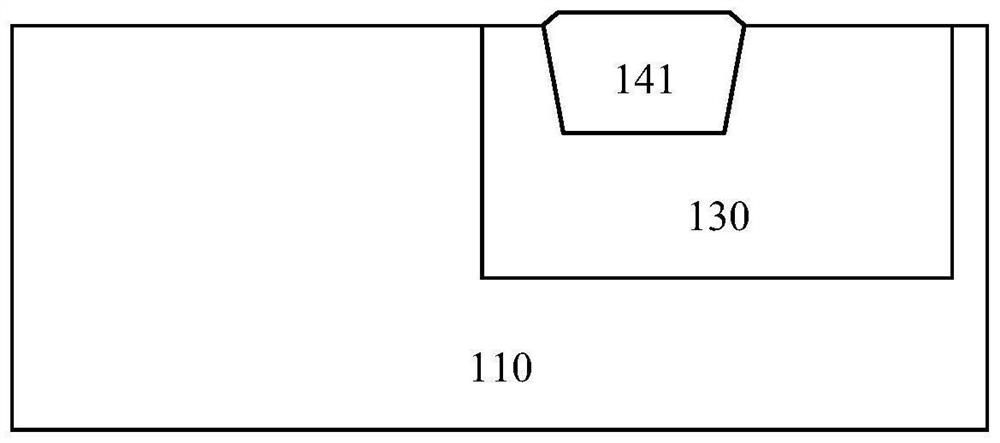
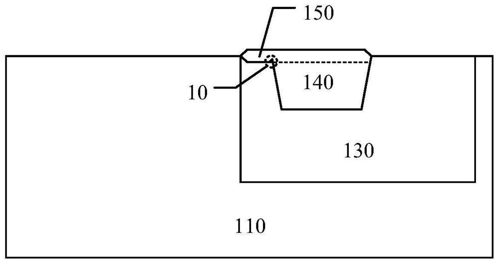
[0033] Figure 2A to Figure 2C A partial process schematic diagram of a manufacturing method of an LDMOS device according to the prior art is shown.

[0034] refer to Figure 2A , in the prior art, a groove is etched at the position of the shallow trench isolation region, and oxide is deposited in the groove to obtain a vertical oxide layer structure 141. In order to ensure the isolation effect, the vertical oxide layer structure 141 The height exceeds the upper surface of the semiconductor sub...


PUM

PropertyMeasurementUnit
angleaaaaaaaaaa

Abstract

According to the semiconductor device and the manufacturing method thereof, after a vertical oxide layer structure is deposited, the upper surface of the vertical oxide layer structure is lowered to be below the upper surface of a semiconductor substrate through etching, and then a horizontal oxide layer structure is obtained through oxidation on the semiconductor substrate and the vertical oxide layer structure according to a local silicon oxidation isolation technology. According to the semiconductor device and the manufacturing method thereof, the upper surface of the vertical oxide layer structure is etched below the upper surface of the semiconductor substrate before the horizontal oxide layer structure is obtained through oxidation, so that the sharp corner structure at the top edge of the groove corresponding to the vertical oxide layer structure can be oxidized from the side surface and the upper surface at the same time during oxidation; the sharp corner structure is smoothed, a smooth junction structure of the horizontal oxide layer structure and the vertical oxide layer structure is obtained, the thickness of the obtained horizontal oxide layer is guaranteed, the breakdown protection performance of the horizontal oxide layer structure is guaranteed, and the performance of the semiconductor device is improved.

Description

technical field [0001] The present invention relates to the field of semiconductor technology, in particular, to a semiconductor device and a manufacturing method thereof. Background technique [0002] The power switch may be a semiconductor device, including a metal-oxide-semiconductor field-effect transistor (Metal-Oxide-Semiconductor Field-Effect Transistor, MOSFET) and an insulated gate bipolar transistor (Insulated Gate Bipolar Transistor, IGBT). Laterally Diffused Metal Oxide Semiconductor (LDMOS) is widely used in switching regulators. [0003] figure 1 shows a schematic structural diagram of an LDMOS device according to the prior art, such as figure 1 As shown, the LDMOS device 100 is provided with a body region 120 and a drift region 130 in a semiconductor substrate 110, a first doped region 121 and a second doped region 122 are arranged in the body region 120, and a drain is arranged in the drift region 130. region 131, a shallow trench isolation (shallow trench...

Claims


Application Information

Patent Timeline
Patent Type & Authority Applications(China)
IPC IPC(8): H01L21/336H01L21/762H01L29/78
CPCH01L29/66681H01L21/76202H01L29/7816H01L21/76235H01L21/76232H01L29/7835H01L21/76224H01L29/7393H01L29/6625H01L29/0834H01L29/0653
Inventor 王欢
Owner SILERGY SEMICON TECH (HANGZHOU) CO LTD
Why Eureka
Try Eureka