Novel clamping structure for clamping Vgs of PMOS

A MOS tube and clamping technology, applied in the field of new clamping structure, can solve the problems of easy leakage, poor clamping effect, and the circuit does not play a big role, and achieves the effect of strong conduction ability

Pending Publication Date: 2022-05-06
SG MICRO
View PDF0 Cites 1 Cited by
  • Summary
  • Abstract
  • Description
  • Claims
  • Application Information

AI Technical Summary

Problems solved by technology

[0004] However, when clamping with a parasitic diode, the size of the MOS tube needs to be considered. If the size of the MOS tube is too small, the clamping effect will be poor and will not play a big role in the subsequent circuits; if the size of the MOS tube is too large, the In some cases, it is easy to leak electricity, which will cause the mismatch of the circuit structure

Method used


Image

  • Novel clamping structure for clamping Vgs of PMOS
  • Novel clamping structure for clamping Vgs of PMOS

Examples


Embodiment Construction

[0029] The application will be further described below in conjunction with the accompanying drawings. The following examples are only used to illustrate the technical solutions of the present invention more clearly, but not to limit the protection scope of the present application.

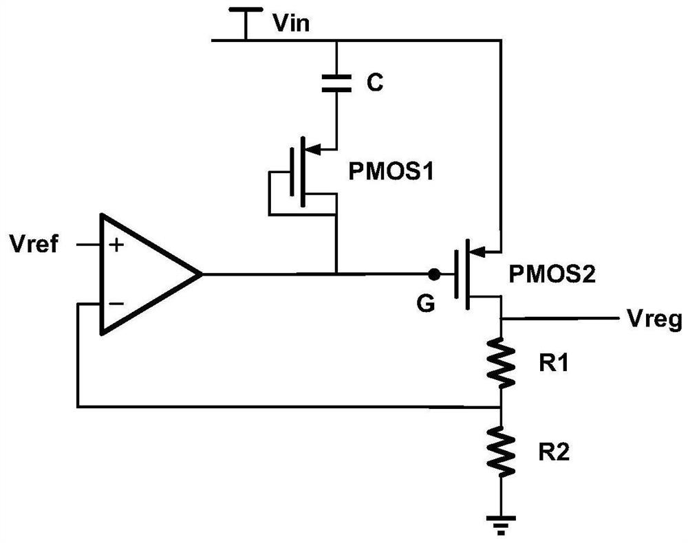
[0030] A novel clamping structure for clamping the Vgs of PMOS according to the present invention, the clamping structure includes a coupling module and a pull-up module;

[0031] The coupling module is connected in series with the pull-up module, wherein one end of the coupling module is connected to the power supply Vin, the other end is connected to one end of the pull-up module, the other end of the pull-up module is connected to the G terminal of the PMOS to be clamped, and the S terminal of the PMOS to be clamped Connect with the power supply Vin, and the D terminal generates Vreg;

[0032] When the power supply Vin rises rapidly, the coupling module turns on the pull-up module, pulls up the...


PUM


Abstract

The invention discloses a novel clamping structure for clamping Vgs of a PMOS. The clamping structure comprises a coupling module and a pull-up module. One end of the coupling module is connected with a power supply Vin, the other end of the coupling module is connected with one end of the pull-up module, the other end of the pull-up module is connected with a G end of a PMOS to be clamped, an S end of the PMOS to be clamped is connected with the power supply Vin, and a D end of the PMOS to be clamped generates Vreg; when the power supply Vin rapidly rises, the coupling module enables the pull-up module to be switched on, the G end of the PMOS to be clamped is pulled up, and the Vgs of the PMOS to be clamped is clamped, so that the Vreg generated by the PMOS to be clamped is stabilized, and the influence on the next stage is reduced. The capacitor and the MOS tube are adopted as a clamping structure, the clamping function is guaranteed through the instantaneous conduction capacity of the MOS tube, the larger the width-to-length ratio of the MOS tube is, the higher the instantaneous capacity is, and the Vgs of the PMOS to be clamped are stable and easy to achieve.

Description

technical field [0001] The invention belongs to the field of integrated circuits or chips, and relates to a novel clamping structure for clamping the voltage Vgs of a PMOS gate relative to a source. Background technique [0002] Inside the high-voltage chip, a stable voltage source Vreg is generated by PMOS, and Vreg can be used as the power supply of the low-voltage working module. When Vin rises rapidly, it is necessary to keep Vreg stable, so as to ensure the working state of the subsequent circuit, even in the case of ESD (electrostatic discharge), Vreg will not become too high, so as to avoid damage to the MOS tube behind. [0003] The scheme adopted in the past is generally: add a diode-connected MOS transistor to Vin at the G terminal of the PMOS (field effect transistor) that generates Vreg, and clamp it with a parasitic diode. Generally, two parasitic diodes are connected in series to ensure the Vgs of the PMOS. It will not change too much due to the fluctuation of...

Claims


Application Information

Patent Timeline
IPC IPC(8): G05F1/56
CPCG05F1/56
Inventor 崔先宇
Owner SG MICRO
Why Eureka
Try Eureka