
Capacitance-based PCB (Printed Circuit Board) for improving integrity of cross-segmentation signal and layout method thereof

A signal integrity, PCB board technology, applied in the direction of printed circuit components, electrical connection formation of printed components, etc., can solve the problems affecting the impedance control of high-speed signal transmission lines, large return path, multi-printed board space, etc., to achieve stability and reliability Data transmission requirements, optimized layout structure, and the effect of reducing the return path

Pending Publication Date: 2022-04-08
SHANGHAI NCATEST TECH CO LTD
View PDF0 Cites 0 Cited by
  • Summary
  • Abstract
  • Description
  • Claims
  • Application Information

AI Technical Summary

Problems solved by technology

[0007] ① Under normal circumstances, the ground around the high-speed signal transmission line will take up more space on the printed board, increasing design and production costs;
[0008] ②. If the high-speed signal transmission line refers to the power layer, there will still be a large return path through the ground wrapping process, and the improvement effect is not obvious;
[0009] ③. After wrapping the ground around the high-speed signal transmission line, the impedance of the high-speed signal transmission line should not only refer to the power supply or ground plane, but also refer to the ground wire around the high-speed signal transmission line. This will affect the impedance control of the high-speed signal transmission line, and the impedance error will be biased. Big;

Method used


Image

  • Capacitance-based PCB (Printed Circuit Board) for improving integrity of cross-segmentation signal and layout method thereof
  • Capacitance-based PCB (Printed Circuit Board) for improving integrity of cross-segmentation signal and layout method thereof

Examples


Embodiment Construction

[0036] The specific embodiment of the present invention will be further described in detail below in conjunction with the accompanying drawings.

[0037] It should be noted that there needs to be a well-designed reference plane in the PCB to obtain the return path, which is a critical stage in the overall design of the circuit board. The method for improving the integrity of the cross-segmented signal based on the capacitance of the present invention can reduce the return path of the high-speed signal, effectively control the sudden change of the impedance of the transmission line, improve the integrity of the transmission signal, and ensure the stable and reliable data transmission of the link.

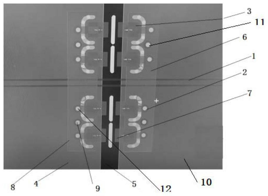
[0038] see figure 2 , figure 2 Shown is a schematic diagram of the layout structure of a printed circuit board that improves signal integrity across divisions based on capacitance according to an embodiment of the present invention. like figure 2 As shown, the PCB board include...


PUM


Abstract

The invention relates to a PCB (Printed Circuit Board) for improving the integrity of a cross-segmentation signal based on a capacitor and a layout method thereof, at least one high-speed transmission signal line is arranged on the PCB, and the high-speed transmission signal line refers to different power supply planes; according to the layout method, two capacitor banks are additionally arranged on the top layer (or the bottom layer) of the PCB, each capacitor bank comprises N capacitors with capacitance values gradually increased from small to large, and the capacitance value of each capacitor is M times of the capacitance value of the previous capacitor. Therefore, according to the design scheme, a backflow path of a high-speed signal can be reduced, impedance abrupt change of the transmission line can be effectively controlled, the integrity of the transmission signal is improved, and stable and reliable data transmission of a link is ensured.

Description

technical field [0001] The present invention relates to the field of semiconductor automatic test equipment (Automatic Test Equipment, referred to as ATE), and in particular to a printed circuit board (PCB) and a layout method for improving the integrity of cross-segmented signals based on capacitance. Background technique [0002] For complex PCB systems, there are usually a large number of high-speed signals. In the PCB layout process of high-speed circuits, in order to reduce costs, there is usually a problem of cross-segmentation. Cross-segmentation may not matter for low-speed transmission signals, but in high-speed transmission digital signal systems, high-speed transmission signals use the reference plane as the return path (return path). If there is a split in the reference plane, the signal reference plane will not be correct. continuous. [0003] That is, when the reference plane is incomplete, cross-segmentation will increase the return path of the signal, result...

Claims


Application Information

Patent Timeline
Patent Type & Authority Applications(China)
IPC IPC(8): H05K1/02H05K3/40
CPCH05K1/02H05K3/40
Inventor 徐涛
Owner SHANGHAI NCATEST TECH CO LTD
Learn More