
Calibration method and system for current density over-standard region of integrated circuit layout

A current density and integrated circuit technology, which is applied in the field of calibration in areas where the current density of the integrated circuit layout exceeds the standard, can solve the problems of inability to accurately obtain useful information, complicated shape of the integrated circuit layout, and calibration methods that are no longer valid.

Active Publication Date: 2022-03-22
北京智芯仿真科技有限公司
View PDF4 Cites 4 Cited by
  • Summary
  • Abstract
  • Description
  • Claims
  • Application Information

AI Technical Summary

Problems solved by technology

[0005] At present, the calibration of the area where the current density exceeds the standard on the integrated circuit layout is usually a rectangular area calibration. This calibration method is effective for the layout shape with a simple structure in the early stage, and can quickly identify the position where the current density exceeds the standard from the calibrated area. The designed layout is optimized and rectified, but as the shape of the integrated circuit layout becomes more and more complex, the original calibration method is no longer effective. Specifically, there are a large number of curved strip layout polygons. If the current density on this polygon According to the traditional calibration method, the over-standard rectangular area including the entire strip layout polygon is included. This rectangular area also contains a large number of layout polygons that do not exceed the standard. Therefore, this calibration is basically invalid and cannot be obtained from Accurately obtain useful information in the marked area

Method used


Image

  • Calibration method and system for current density over-standard region of integrated circuit layout
  • Calibration method and system for current density over-standard region of integrated circuit layout
  • Calibration method and system for current density over-standard region of integrated circuit layout

Examples


Embodiment Construction

[0089] The application will be further described below in conjunction with the accompanying drawings. The following examples are only used to illustrate the technical solutions of the present invention more clearly, but not to limit the protection scope of the present application.

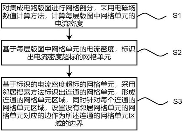
[0090] In the first aspect, this application proposes a method for calibrating the region where the current density of the integrated circuit layout exceeds the standard, such as figure 1 shown, including the following steps:

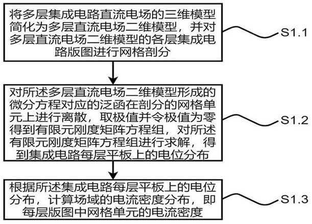
[0091] Step S1: performing grid division on the layout of the integrated circuit, and calculating the current density of the grid cells in each layout layer by using the electromagnetic field numerical calculation method;

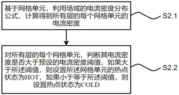
[0092] Step S2: Based on the current density of the grid cells in each layout layer, identify the grid cells whose current density exceeds the standard;

[0093] Step S3: Based on the grid cells whose identified current density exceeds the standard, us...


PUM


Abstract

The invention discloses an integrated circuit layout current density exceeding area calibration method and system, and belongs to the technical field of integrated circuit electromagnetic field analysis, and the method comprises the steps: carrying out the mesh generation of an integrated circuit layout, employing an electromagnetic field numerical calculation method, and calculating the current density of a mesh unit in each layer of layout; based on the current density of the grid units in each layer of layout, identifying the grid units with the current density exceeding the standard; and identifying connected grid cells by adopting a neighbor search method based on the identified grid cells with the current density exceeding the standard to form connected grid cell regions, and setting edges corresponding to the grid cells without neighbor grid cells as boundaries of the connected grid cell regions for each connected grid cell region. The current density calibration method solves the problems that when the layout shape of the integrated circuit is complex, a traditional current density calibration method is not effective any more, and a current density exceeding area cannot be accurately calibrated, and is beneficial to optimization and rectification of the layout of the large-scale integrated circuit.

Description

technical field [0001] The application belongs to the technical field of integrated circuit electromagnetic field analysis, and in particular relates to a method and system for calibrating an area where the current density of an integrated circuit layout exceeds the standard. Background technique [0002] With the development of communication technology, the research and development of VLSI has gradually started. In order to improve the performance of electronic equipment, reduce the size and reduce the cost, the current production status is to integrate transistors, other components and circuits on a small semiconductor substrate. In order to achieve more functions, VLSIs currently have several to hundreds of layers of structures, each layer is extremely complex, and integrates tens of millions or even hundreds of millions of transistors, and all of them have centimeter-level to the latest nano-level Multiscale structure. Such a complex structure also brings difficulties ...

Claims


Application Information

Patent Timeline
Patent Type & Authority Applications(China)
IPC IPC(8): G06F30/392G06F30/23G06F111/10
CPCG06F30/392G06F30/23G06F2111/10
Inventor 王芬
Owner 北京智芯仿真科技有限公司
Learn More