Wafer fixing device and wafer drying device

A wafer fixation and wafer technology, which is applied in drying chamber/container, dryer, semiconductor/solid-state device manufacturing, etc., can solve the problems of poor drying effect of wafers, enhance the ability to absorb particulate matter, and ensure The effect of the drying effect

Pending Publication Date: 2022-03-11
HWATSING TECH
View PDF0 Cites 1 Cited by
  • Summary
  • Abstract
  • Description
  • Claims
  • Application Information

AI Technical Summary

Problems solved by technology

Under some working conditions, the particles at the contact between the jaws and the wafer usually adhere to the side of the jaws due to the capillary effect, and the fluid cannot be quickly drained from the engaging part of the jaws, resulting in poor drying of the wafers

Method used


Image

  • Wafer fixing device and wafer drying device
  • Wafer fixing device and wafer drying device
  • Wafer fixing device and wafer drying device

Examples


Embodiment Construction

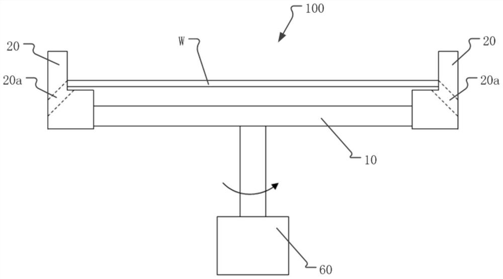
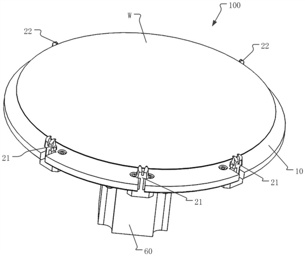
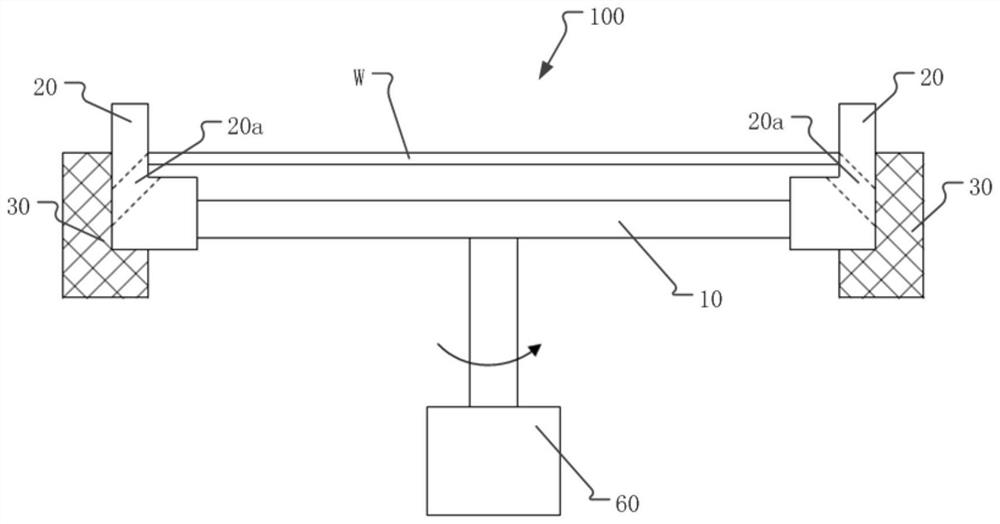
[0031] The technical solutions of the present invention will be described in detail below in conjunction with specific embodiments and accompanying drawings. The examples described here are specific implementations of the present invention and are used to illustrate the concept of the present invention; these descriptions are all explanatory and exemplary, and should not be construed as limiting the implementation of the present invention and the protection scope of the present invention . In addition to the embodiments described here, those skilled in the art can also adopt other obvious technical solutions based on the claims of the application and the contents disclosed in the specification, and these technical solutions include adopting any modifications made to the embodiments described here. Obvious alternatives and modified technical solutions.

[0032] The accompanying drawings in this specification are schematic diagrams, which assist in explaining the concept of the...


PUM


Abstract

The invention discloses a wafer fixing device and a wafer drying device.The wafer fixing device comprises a bottom supporting piece, a plurality of clamping jaws are arranged on the peripheral side of the bottom supporting piece at intervals, and clamping parts used for abutting against the edge of a wafer are formed on the clamping jaws; the clamping jaw is provided with a dredging hole, and the dredging hole is formed in a penetrating mode from the clamping portion of the clamping jaw to the outer side. The dredging holes can guide fluid to be discharged so as to restrain the fluid from staying at the wafer or the clamping jaw.

Description

technical field [0001] The invention belongs to the technical field of wafer post-processing, and in particular relates to a wafer fixing device and a wafer drying device. Background technique [0002] Chemical Mechanical Polishing (CMP) is an ultra-precision surface processing technology for global planarization in integrated circuit (Integrated Circuit, IC) manufacturing. With the development of integrated circuit manufacturing technology, the control of wafer surface defects is becoming more and more stringent. During the wafer manufacturing process, the surface of the wafer will absorb pollutants such as particles or organic matter to generate a large number of defects, which require post-processing to remove these defects. In particular, chemical reagents and abrasives used in large quantities in chemical mechanical polishing will cause contamination on the surface of the wafer, so after polishing, a post-treatment process is required to remove pollutants on the surfac...

Claims


Application Information

Patent Timeline
Patent Type & Authority Applications(China)
IPC IPC(8): H01L21/687H01L21/67B08B3/02F26B25/18
CPCH01L21/68785H01L21/68728H01L21/67034B08B3/02F26B25/18
Inventor 李长坤曹自立
Owner HWATSING TECH
Why Eureka
Try Eureka